This project describes how to control an RGB LED using an Android application via Bluetooth.
Below we described steps needed to understand how the solution has been programmed to create the RBG LED color control. However, if you just want to get the result of programming, download GreenPAK™ software to view the already completed GreenPAK Design File. Plug the GreenPAK Development Kit to your computer and hit the program to design the solution.
Introduction
Smart bulbs have been increasing in popularity recently and are steadily becoming a key part of the smart home toolkit. Smart bulbs enable the user to control their light via a special application on the user’s smart phone; the bulb can be turned on and off and the color can be changed from the application interface. In this project, we built a smart bulb controller that can be controlled from a manual button or a mobile application via Bluetooth. To add some flair to this project we have added some features which allow the user to choose a lighting color from the list of colors included in the application interface. It can also activate an “auto mix” to generate color effects and change the lighting every half second. The user can create their own color mix using a PWM feature which can also be used as a dimmer for the three basic colors (red, green, blue). We also added external buttons to the circuit so that the user can switch to manual mode and change the light color from an external button.
This application is comprised of two sections; the GreenPAK design and Android app design. The GreenPAK design is based on using a UART interface for communication. UART is chosen because it is supported by most Bluetooth modules, as well as most other peripherals, such as WIFI modules. Consequently, the GreenPAK design can be used in many connection types.
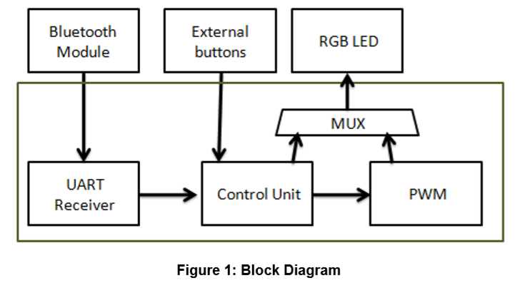
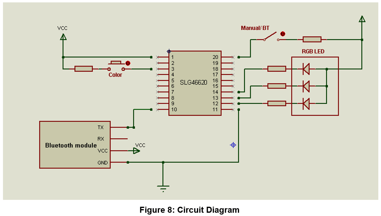
To build this project, we are going to use the SLG46620 IC, a Bluetooth module, and an RGB LED. The GreenPAK IC is going to be the control core of this project; it receives data from a Bluetooth module and/or external buttons, then begins the required procedure to display the correct lighting. It also generates the PWM signal and outputs it to the LED. Figure 1 below shows the block diagram.
The GreenPAK device used in this project contains a SPI connection interface, PWM blocks, FSM and a lot of other useful additional blocks in one IC. It is also characterized by its small size and low energy consumption. This will enable manufacturers to build a small practical circuit using a single IC, thus the production costs will be minimized when compared to similar systems.
In this project, we control one RGB LED. To make the project commercially viable, a system would likely need to increase the luminosity level by connecting many LEDs in parallel and using the appropriate transistors; the power circuit needs to be taken into consideration as well.
This project was implemented and examined; you can watch the video of the project that shows the in-depth behavior of the circuit.
GreenPAK Design
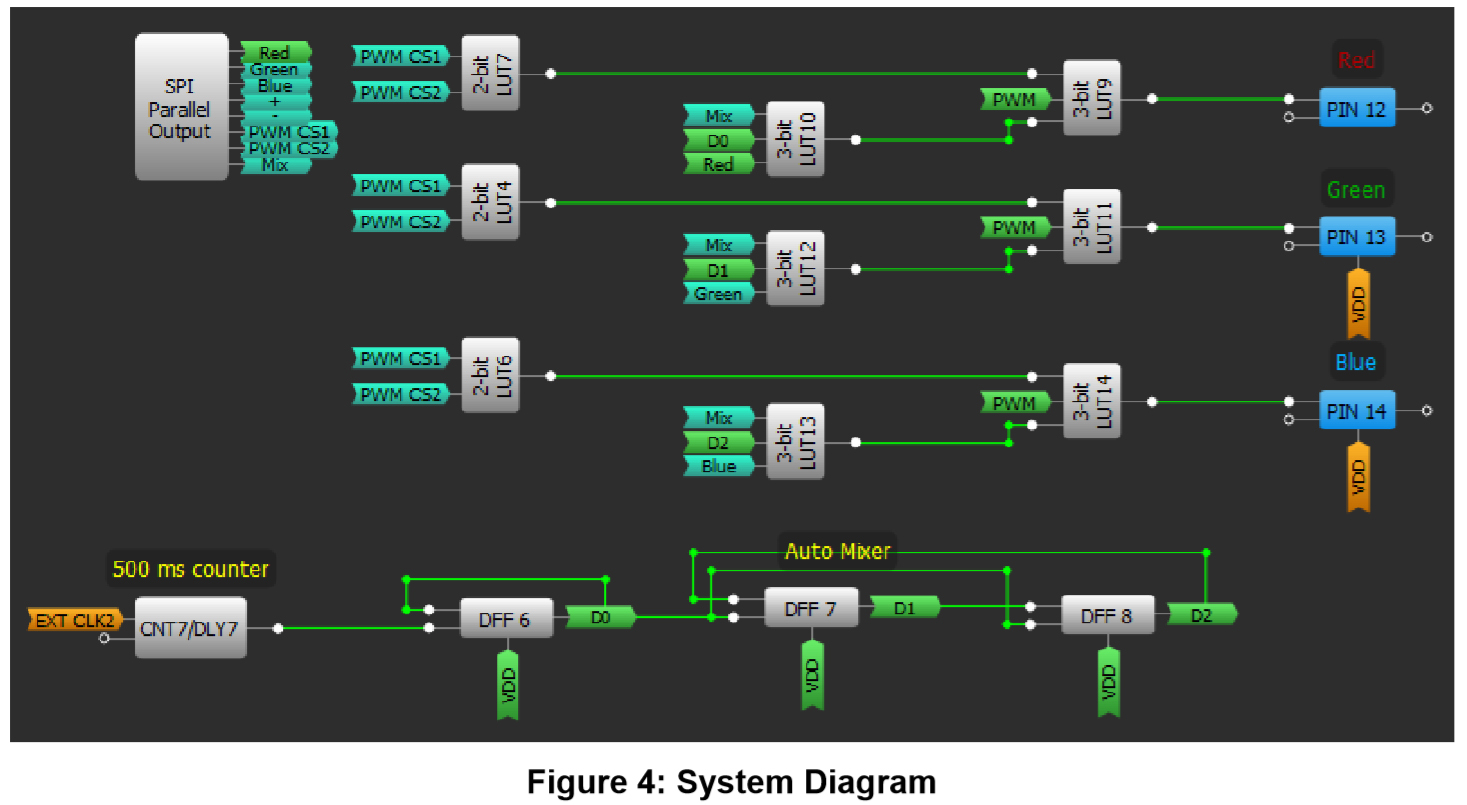
The GreenPAK design consists of the UART receiver, PWM unit, and control unit.
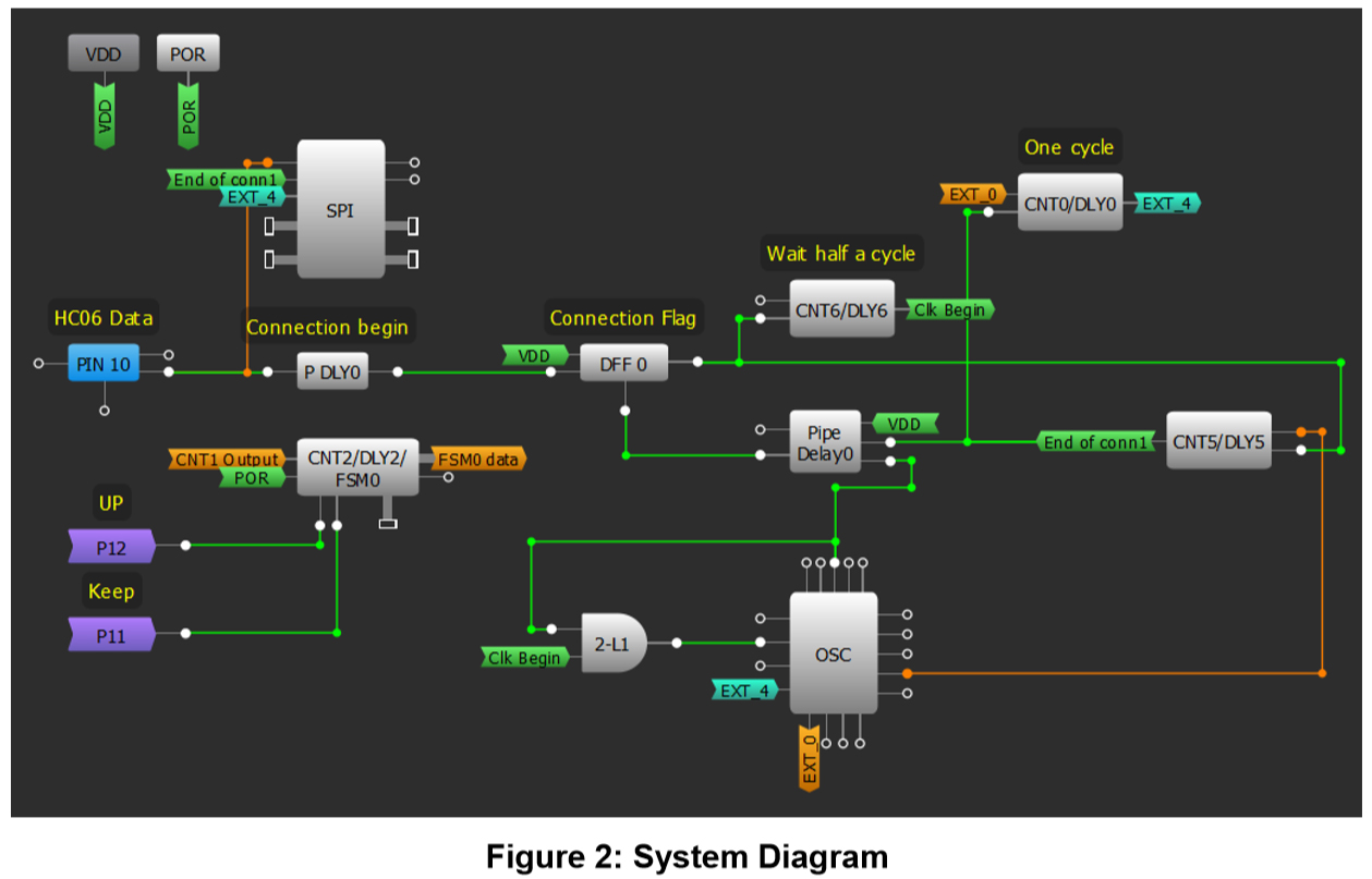
First, we need to set up the Bluetooth module. Most Bluetooth ICs support the UART protocol for communication. UART stands for Universal Asynchronous Receiver / Transmitter. UART can convert data back and forth between parallel and serial formats. It includes a serial to parallel receiver and a parallel to serial converter which are both clocked separately.
The data received in the Bluetooth module will be transmitted to our GreenPAK device. The idle state for Pin10 is HIGH. Every character sent begins with a logic LOW start bit, followed by a configurable number of data bits and one or more logic HIGH stop bits.
The UART transmitter sends 1 START bit, 8 data bits, and one STOP bit. Usually, the default baud rate for a UART Bluetooth module is 9600. We will send the data byte from the Bluetooth IC to the GreenPAK SLG46620’s SPI block.
Since the GreenPAK SPI block does not have START or STOP bit control, we will use those bits instead to enable and disable the SPI clock signal (SCLK). When Pin10 goes LOW, we know we have received a START bit, so we use the PDLY falling edge detector to identify the start of communication. That falling edge detector clocks DFF0, which enables the SCLK signal to clock the SPI block.
Our baud rate is 9600 bits per second, so our SCLK period needs to be 1/9600 = 104 μs. Therefore, we set the OSC frequency to 2MHz and used CNT0 as a frequency divider.
2 MHz-1 = 0.5 μs
(104 μs / 0.5 μs) - 1 = 207
Therefore, we want the CNT0 counter value to be 207. To ensure that we don’t miss any data, we need to delay the SPI clock by half a clock cycle so that the SPI block is being clocked at the proper time. We accomplished this by using CNT6, 2-bit LUT1, and the OSC block’s External Clock. The output of CNT6 does not go high until 52 μs after DFF0 is clocked, which is half of our 104 μs SCLK period. When CNT6 is high the 2-bit LUT1 AND gate allows the 2MHz OSC signal to pass into the EXT. CLK0 input, whose output is connected to CNT0.
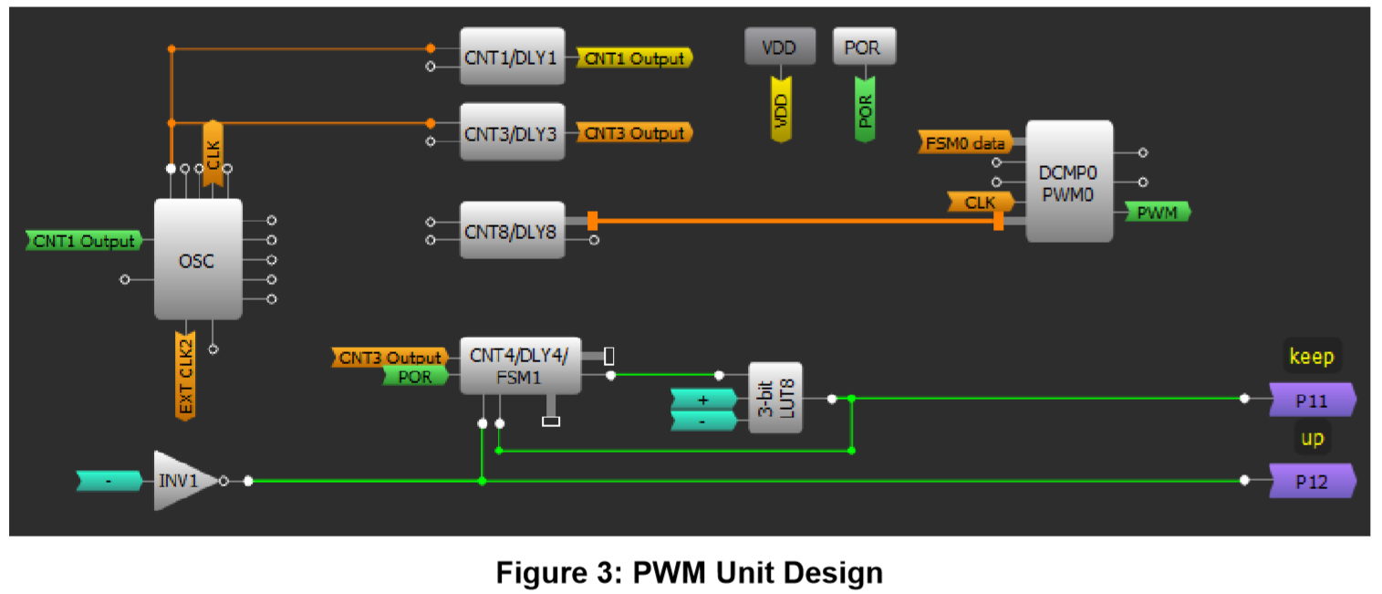
The PWM signal is generated using PWM0 and an associated clock pulse generator (CNT8/DLY8). Since the pulse width is user-controllable, we use FSM0 (which can be connected to PWM0) to count user data.
In the SLG46620, 8-bit FSM1 can be used with PWM1 and PWM2. The Bluetooth module must be connected, which means the SPI parallel output must be used. The SPI parallel output bits 0 through 7 are muxed with DCMP1, DMCP2, and the LF OSC CLK’s OUT1 and OUT0. PWM0 obtains its output from the 16-bit FSM0. Left unaltered this causes the pulse width to overload. To limit the counter value at 8 bits another FSM is added; FSM1 is used as a pointer to know when the counter reaches either 0 or 255. FSM0 is used to generate the PWM pulse. FSM0 and FSM1 must be synchronized. Since both FSMs have preset clock options, CNT1 and CNT3 are used as mediators to pass the CLK to both FSMs. The two counters are set to the same value, which is 25 for this project. We can alter the rate of change of the PWM value by changing these counter values.
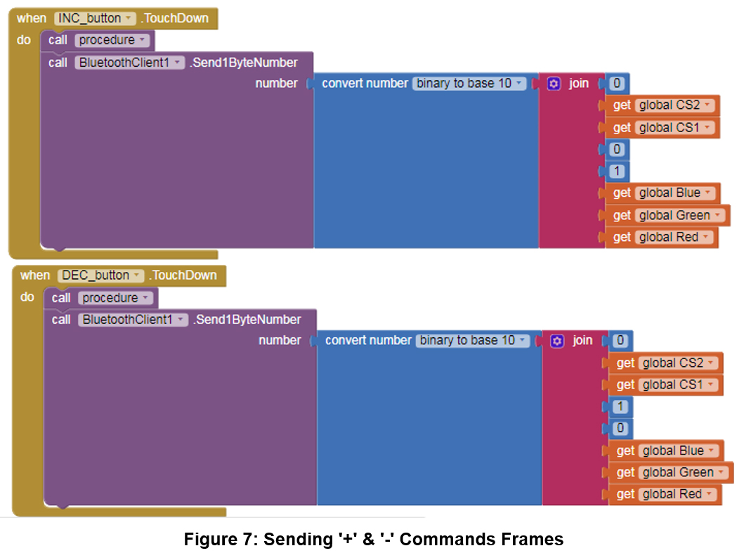
The value of the FSMs are increased and decreased by the signals '+' and '-', which originate from the SPI Parallel Output.
Within the control unit the received byte is taken from the Bluetooth module to the SPI Parallel Output and is then passed to the associated functions. At first, PWM CS1 and PWM CS2 outputs will be checked to see if the PWM pattern is activated or not. If it is activated then it will determine which channel is going to output the PWM through LUT4, LUT6, and LUT7.
LUT9, LUT11, and LUT14 are responsible for checking the state of the other two LEDs. LUT10, LUT12, and LUT13 check whether the Manual button is activated or not. If Manual mode is active, then the RGB outputs operate according to the D0, D1, D2 output states, which are changed every time the Color button is pressed. It changes with the rising edge coming from CNT9, which is used as a rising edge debouncer.
Pin 20 is configured as an input and is used to switch between Manual and Bluetooth control.
If Manual mode is disabled and Auto mixer mode is activated, then the color changes every 500ms with the rising edge coming from CNT7. A 4-bit LUT1 is used to prevent '000' state for D0 D1 D2, since this state causes the light to turn off during Auto mixer mode.
If the Manual mode, PWM mode, and the Auto mixer mode are not activated then the red, green and blue SPI commands flow to Pins 12, 13 and 14, which are configured as outputs and are connected to the external RGB LED.
DFF1, DFF2 and DFF3 are used to build a 3-bit binary counter. The counter value increases with CNT7 pulses that pass through P14 in Auto mixer mode, or from signals coming from the Color button(PIN3) in manual mode.
Android Application
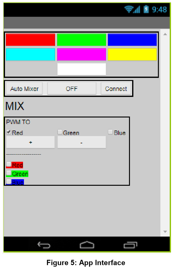
In this section, we are going to build an Android application that will monitor and display the user’s control selections. The interface consists of two sections: the first section contains a set of buttons which have predefined colors so that when any of these buttons is pressed, a LED of the same corresponding color is lit. The second section (MIX square) creates a mixed color for the user.
In the first section, the user chooses the LED pin that they want the PWM signal to pass through; the PWM signal can only be passed to one pin at a time. The lower list controls the other two colors logically on/off during the PWM mode.
The auto mixer button is responsible for running the automatic light changing pattern where the light will change every half second. The MIX section contains two checkbox lists so that the user can decide which two colors to mix together.
We built the application using the MIT app inventor website. It is a site that allows building Android applications without prior software experience using graphical software blocks.
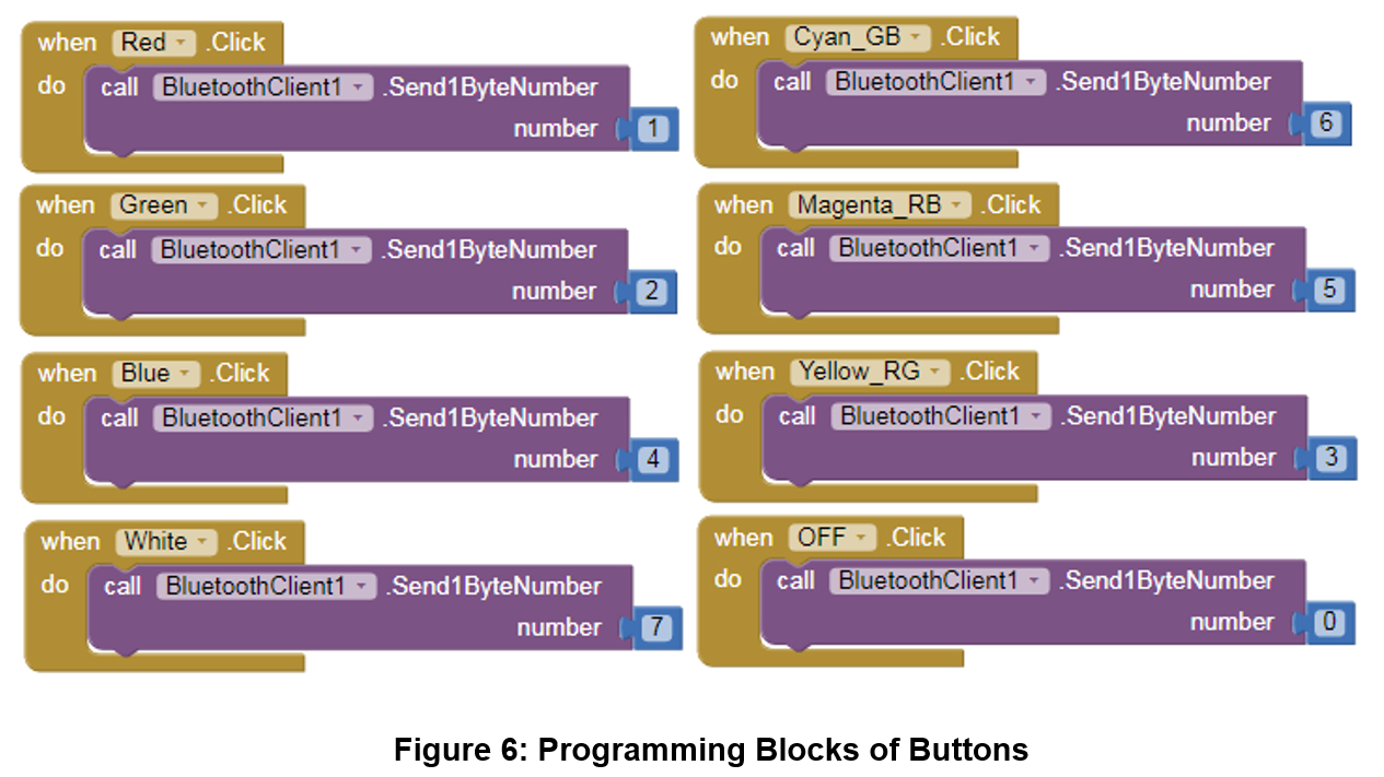
At first, we designed a graphical interface by adding a set of buttons responsible for displaying the predefined colors, we also added two check box lists, and each list has 3 elements; each element is outlined in its individual box, as shown in Figure 5.
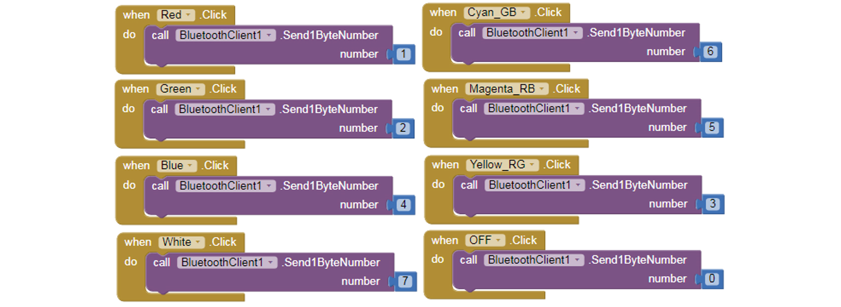
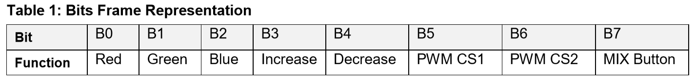
The buttons within the user interface are linked to software commands: all the commands that the app will send via Bluetooth will be in byte format, and each bit is responsible for a specific function. Table 1 shows the form of the command frames sent to the GreenPAK.
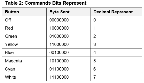
The first three bits, B0, B1 and B2, will hold the state of RGB LEDs in the direct controlling mode by the buttons of the predefined colors. Thus, when clicking on any of them, the corresponding value of the button will be sent, as shown in Table 2.
The bits B3 and B4 hold the '+' and '-' commands, which are responsible for increasing and decreasing pulse width. When the button is pressed the bit value will be 1, and when the button is released the bit value will be 0.
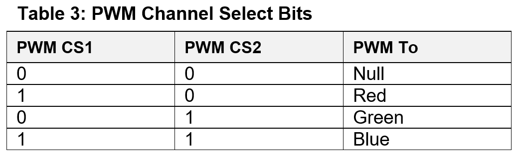
The B5 and B6 bits are responsible for choosing the pin (color) that the PWM signal will pass through: the color designations of these bits are shown in table 3. The last bit, B7, is responsible for activating the auto mixer.
Figure 6 and Figure 7 demonstrate the process of linking buttons with programming blocks which are responsible for sending the previous values.
To watch the full design of the application, you can download the attached file “.aia” with the project files and open it within the main site.
Figure 8 below shows the top level circuit diagram.
Results
The Controller was tested successfully and the color mixing, along with other features, were shown to work appropriately.
Conclusion
In this project, a smart bulb circuit was built to be wirelessly controlled by an Android application. The GreenPAK IC used in this project also helped to shorten and embed several essential components for light control into one small IC.