Check outhow to create a voice-activated Smart Home controller
Below we described steps needed to understand how the solution has been programmed to create the smart home controller. However, if you just want to get the result of programming, download GreenPAK™ Designer software to view the already completed GreenPAK Design File. Plug the GreenPAK Development Kit to your computer and hit the program to design the device.
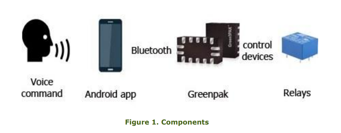
This project shows how to create a voice-activated Smart Home controller. It involves creating a simple Android App and interfacing with a Bluetooth node, which is connected to several smart electrical outlets.
This design is implemented with an SLG46620V GreenPAK device, an HC06 Bluetooth module, and a few relays.
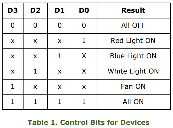
We will use this design to control four electrical devices: a red light, a blue light, a white light, and a fan. Each of these devices can either be ON or OFF.
Android Application
This Android Application will be able to receive voice commands, convert them into a command, and send the commands to the Bluetooth module to be carried out.
This app was made with MIT App Inventor, which doesn’t require any programming experience. The App Inventor lets the developer create an application for Android OS devices using a web browser by connecting programming blocks.
Since each of our four devices can either be ON or OFF, we need four bits to represent all the possible states for each of the devices.
Table 1 illustrates the control bits for each of our four devices. In the table, “x” denotes a bit that we do not wish to change, so we keep it unchanged. Each bit represents a device state, where 1 = ON, and 0 = OFF.
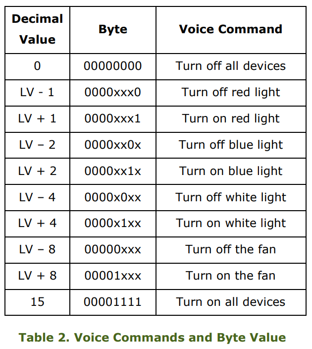
Since our application includes voice controls, we need to define what phrases will generate a command to our system.
Table 2 shows which voice commands will turn on or off each device. In the first column, LV stands for Last Value, i.e. the previous byte value that was sent. Since the red light is controlled by the least significant bit in our byte, if we add 1 to the previous byte value it will turn the red light ON. Likewise, if we subtract 1 from the previous byte value it will turn the red light OFF.
You can import our App into the MIT App Inventor by clicking on “Projects” -> “Import project (.aia) from my computer”, and selecting the .aia file included with this project.
To create the Android Application, we need to start a new project and remove the visible components from the designer screen. Then we need to create two buttons: the first is a list picker for Bluetooth devices, and the second is a button to begin voice recognition.
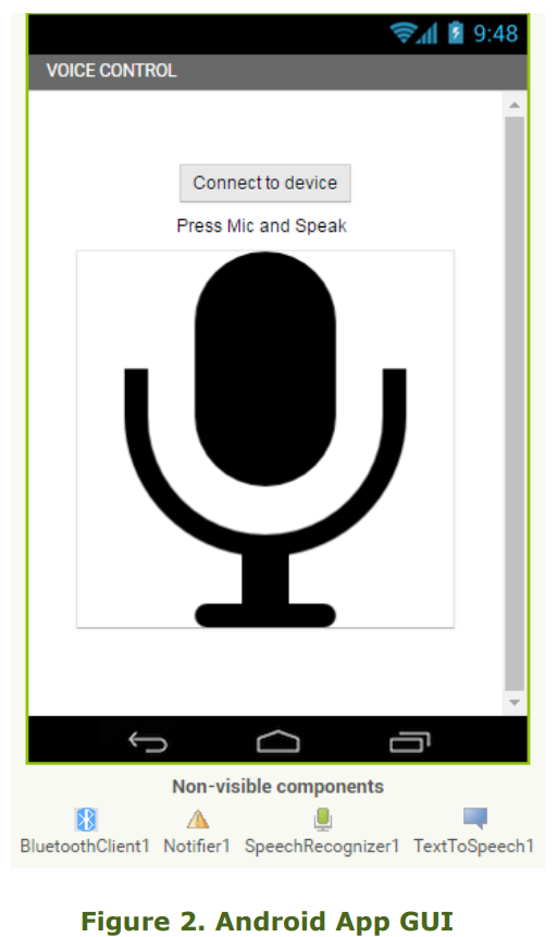
Other components we need to add include a Bluetooth client, speech recognition, and text-to-speech modules. Figure 2 below is a screen capture of our Android Application’s user interface.
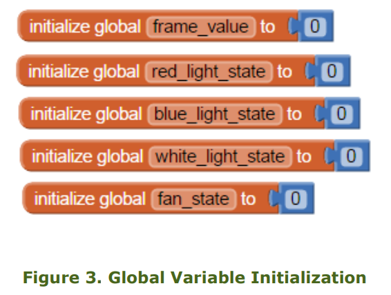
We can now start programming by clicking on the “Block” button. We can add components by dragging and dropping from the bar on the left. We will start by adding our global variables, as shown in Figure 3.
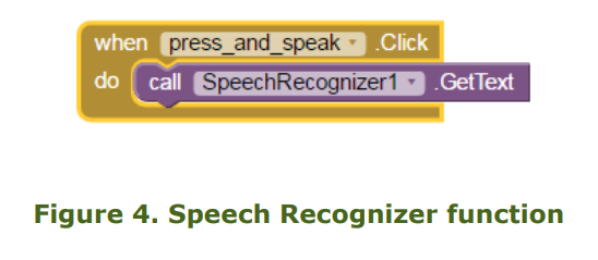
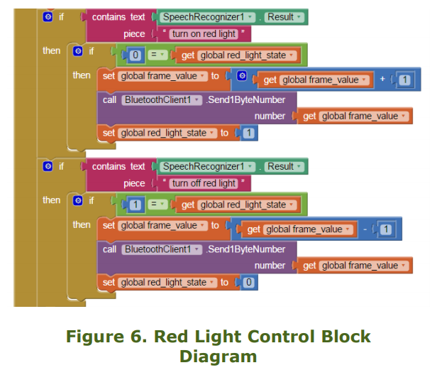
Now we can add the voice recognition block that will be called when the user presses the large microphone button.
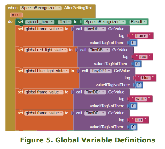
The text received by this function will be interpreted to determine which command to send to our Bluetooth module. Figure 6 on page 3 shows the full block diagram for our “Turn on red light” and “Turn off red light” commands.
Gathering Data from Bluetooth Module
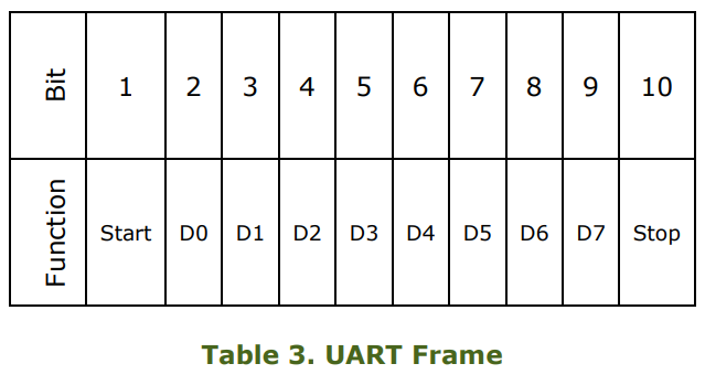
Now that we have our Android Application ready, we need to set up our HC06 Bluetooth module. The HC06 uses the UART protocol for communication.
UART stands for Universal Asynchronous Receiver / Transmitter. UART can convert data back and forth between parallel and serial formats. It includes a serial to parallel receiver and a parallel to serial converter which are both clocked separately.
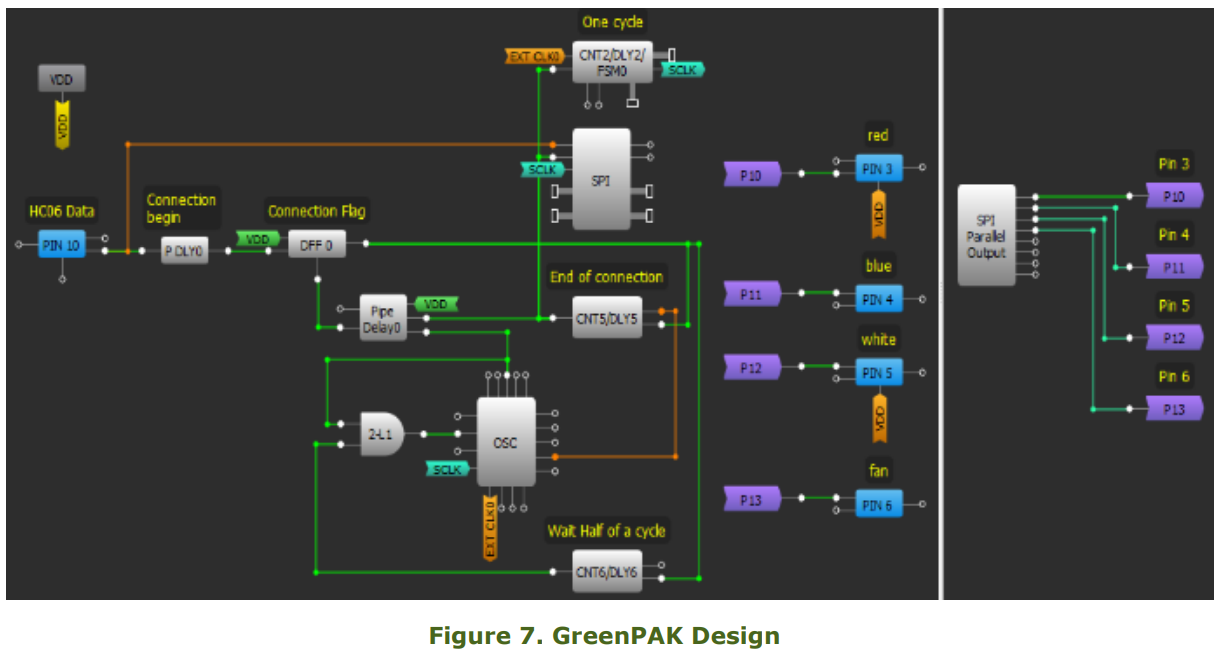
The data received in the HC06 will be transmitted to our GreenPAK device.
GreenPAK Design
The idle state for Pin10 is HIGH. Every character sent begins with a logic LOW start bit, followed by a configurable number of data bits, and one or more logic HIGH stop bits.
The HC06 sends 1 START bit, 8 data bits, and one STOP bit. Its default baud rate is 9600. We will send the data byte from the HC06 to the GreenPAK SLG46620’s SPI block.
Since the SPI block does not have START or STOP bit control, we will use those bits instead to enable and disable the SPI clock signal (SCLK). When Pin10 goes LOW, we know we have received a START bit, so we use the PDLY falling edge detector to identify the start of communication. That falling edge detector clocks DFF0, which enables the SCLK signal to clock the SPI block.
Our baud rate is 9600 bits per second, so our SCLK period needs to be 1/9600 = 104µs. Therefore, we set the OSC frequency to 2MHz and used CNT2 as a frequency divider.
2MHz-1 = 0.5µs
(104µs / 0.5µs) - 1 = 207
Therefore, we want the CNT2 counter value to be 207. To ensure that we don’t miss any data, we need to delay the SPI clock by half a clock cycle so that the SPI block is being clocked at the proper time. We accomplished this by using CNT6, 2-bit LUT1, and the OSC block’s External Clock. The output of CNT6 does not go high until 52µs after DFF0 is clocked, which is exactly half of our SCLK period of 104µs. When it goes high, the 2-bit LUT1 AND gate allow the 2MHz OSC signal to pass into the EXT. CLK0 input, whose output is connected to CNT2.
Pipe Delay0 is used to reset DFF0 after all of the data has been received.
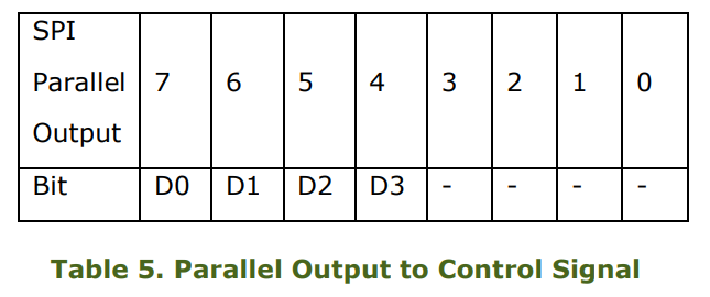
Now that the command has been received by the GreenPAK, it needs to be output via the SPI Parallel Output block.
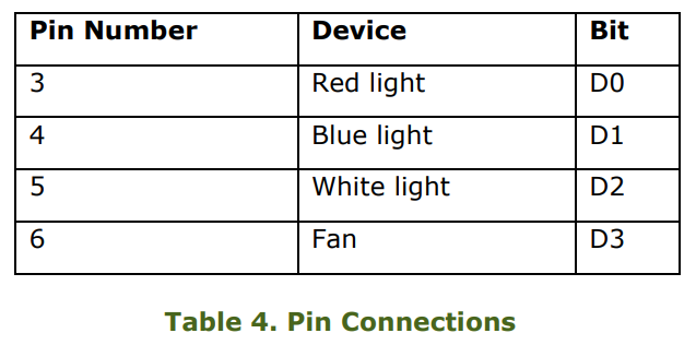
Since the SLG46620V is a dual-matrix chip, we need to use the purple cross-matrix connections to send the four signals from the SPI Parallel Output block back to the other side of the chip so that they can be connected to Pins 3, 4, 5, and 6.
One difference between the UART and SPI communication protocols is the order in which the bits are sent. SPI sends the MSB first, while UART sends the LSB first. This means that our LSB will be taken from the SPI Parallel Output block’s MSB pin.
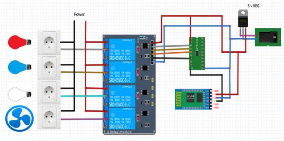
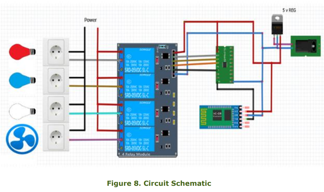
Circuit Schematic
Figure 8 is a schematic of the overall circuit. We used a 5v regulator to step down a 12v input voltage to power our GreenPAK chip and the HC06 Bluetooth module.
As you can see, the HC06’s TX pin is connected to the GreenPAK’s Pin10. The GreenPAK’s Pin3, Pin4, Pin5, and Pin6 are connected to the relay control pins, and the output of each relay is connected to its respective socket.
Conclusion
In this project, we created a homemade Smart Home Controller with an Android Application, an HC06 Bluetooth module, a GreenPAK SLG46620V, and several relays. This Smart Home Controller allows the user to control several outlets with a simple spoken phrase.
The GreenPAK Programmable Mixed-Signal ASICs have a variety of digital and analog components that facilitate the creation of moderately complex designs. GreenPAK IC’s allow the user to easily integrate several discrete components into a single small chip.