This project describes how to use a GreenPAK to automatically set an amplifier bias circuit.
Below we described steps needed to understand how the solution has been programmed to create the automatic amplifier bias control. However, if you just want to get the result of programming, download GreenPAK™ Designer software to view the already completed GreenPAK Design file. Plug the GreenPAK Development Kit into your computer and hit the program to design the device.
Dialog’s programmable mixed signal GreenPAK ASICs are an ideal product to use when configurable and flexible control circuits are desired. This project will detail using a GreenPAK to automatically set an amplifier bias circuit.
Background Concept
It usually is desired to operate the amplifier at as low a power level as necessary. This saves power consumption, reduces heat, increases reliability, etc. At times a higher power level may be desired due to the radio link being insufficient. Developing a circuit to handle his can be complex and have multiple external components. Using a Dialog GreenPAK IC, the designer can easily use a single component to provide the needed voltages and control circuits to the amplifier as well as provide useful alarm and monitoring functions.
This project assumes operation at 900 MHz and will use the following devices as examples:
● GreenPAK: Dialog SLG46582V
● Amplifier: Mini-Circuits PHA-23LNB+
● LNA: Mini-Circuits TSY-13LNB+
● Digital Step Attenuator: Skyworks SKY12325-35-LF
● Detector Diode: Skyworks SMS3923-079LF
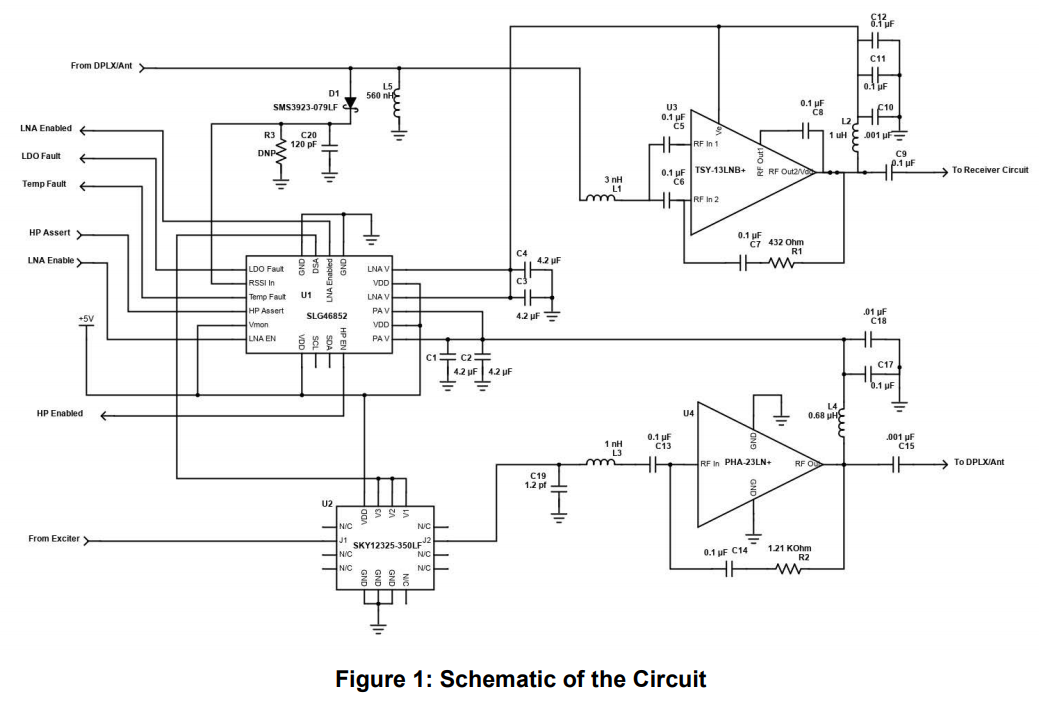
The GreenPAK control circuit will provide two bias voltages to the PHA-23LNB+ and control input signal attenuation to the amp depending on received signal conditions and will also optionally enable the TSY-13LNB+ LNA with Bypass. The schematic of the circuit is shown in Figure 1.
Detector Circuit
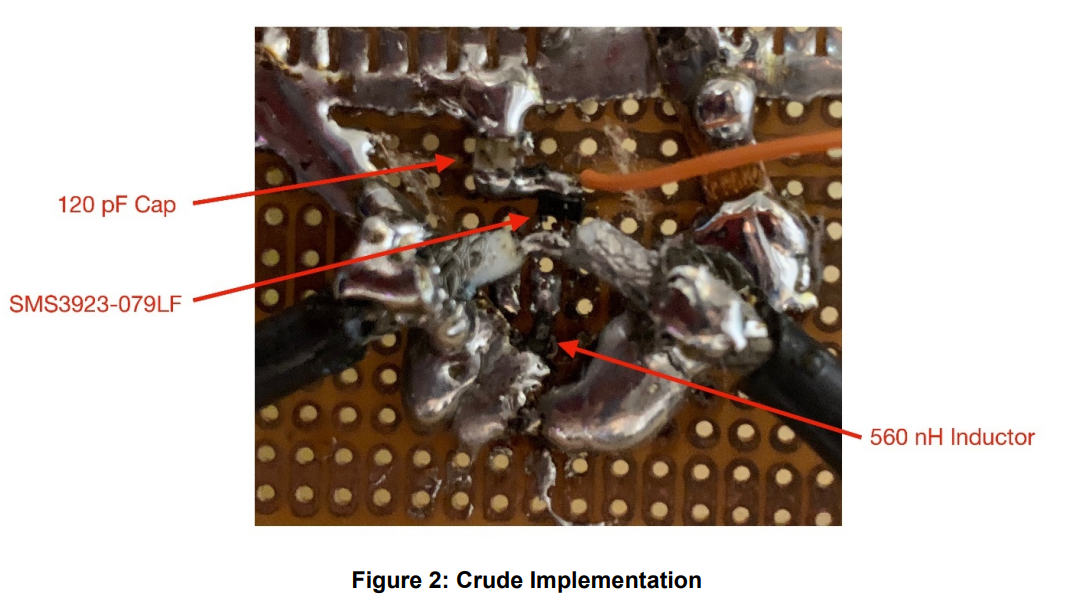
In this example, a Schottky detector diode is used to measure the RF signal being received at the antenna of the radio. The diode used in this design is a Skyworks SMS3923-079LF. The circuit design is quite basic and could likely be improved upon. RF is rectified across the junction of the diode. Any remaining RF on the anode side of the diode is shunted to ground by the 120 pF capacitor. Any DC appearing on the cathode side of the diode will be shorted to ground by the 560 nH inductor. Resistor R3 in the schematic was not used in this example. The circuit as designed outputs about 110 mV DC with approximately 0 dB input. A picture of a crude implementation is shown in Figure 2.
The output from this circuit is fed into the RSSI input pin on the GreenPAK IC. When the voltage in the RSSI pin drops sufficiently (50 mV in this example), the GreenPAK will adjust the bias point of the amplifier and increase the power supplied to the amplifier to improve performance. When the received signal is sufficiently strong, the bias point will be reduced thereby saving power.
Improvements made to this circuit could include using forward bias across the diode to improve voltage output. A better and cleaner layout would also result in improved performance. Additionally, an amplifier could be used to increase the level of voltage output.
Power Amplifier
The PHA-23LN+ MMIC amplifier from Mini-Circuits was chosen because it has very good performance in both gain and output power at two voltage levels: 3 V and 5 V. At 3 V the amplifier biases at 72.4 mA of with ~ 20 dB of gain and P1dB ~ +19 dBm. At 5 V, the amplifier biases at 141.7 mA with ~ 21 dB of gain and P1dB ~ +24 dBm. In this design, the PHA-23LN+ amplifier will be biased at 3 V in low power mode and 5 V in high power mode. A regulated 5 V supply will be required.
Digital Step Attenuator
In this example, a digital step attenuator is used to control the amount of RF power being delivered to the amplifier. This could be used in a real-world circuit, or a microprocessor could be used to control the output of an RF chipset. The Skyworks SKY12325-350LF is a 3-bit, 7 dB digital step attenuator. When all 3 bits are at logic low, the attenuator is at maximum attenuation. At logic high, the attenuator is at minimum attenuation.
Low Noise Amplifier
The TSY-13LNB+ from Mini-Circuits is an LNA with bypass and extremely low current consumption. At 2.7 V bias, the amplifier has about 1.4 dB NF, 14 dB gain with about 7.7 mA current consumption. When the bias is removed, the bypass feature of the amplifier is enabled with minimal insertion loss (about -1.8 dB). The GreenPAK bias controller IC has an LNA enable pin that allows a microprocessor or other control device to enable the LNA switching feature if so desired. If this is not enabled, the LNA will always be turned off and in bypass mode.
SLG46582V GreenPAK Schematic
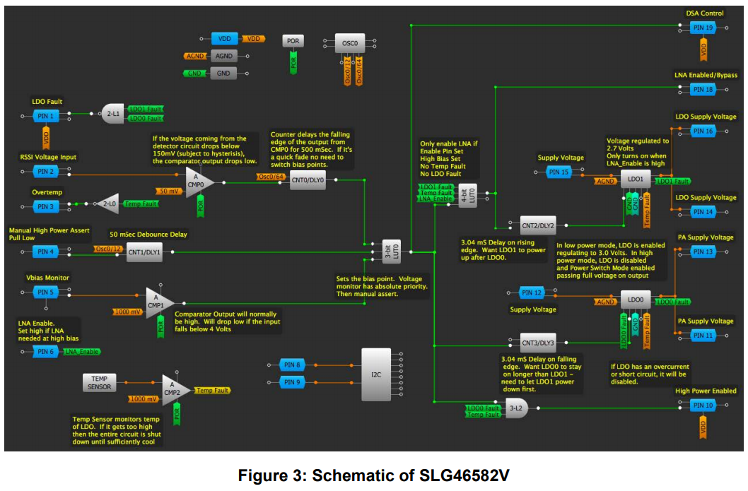
Internally, the schematic of the SLG46582V is shown in Figure 3. The explanation of the circuit functions will follow.
IC Circuit Features
Voltage Monitoring: The supply voltage to the IC must be greater than 4 V in order for the circuit to switch power states. This feature was implemented so that battery powered designs will conserve remaining battery power if the battery voltage begins to drop.
Temperature Monitoring: The SLG46852 features an on-board temperature sensor. If the temperature of the devices exceeds approximately 95 °C, the entire circuit will be turned completely off. Once the IC die cools sufficiently, the temperature fault will clear and the LDOs will be re-enabled at their proper operating state. Pin 3 of the SLG46582 has been configured to allow monitoring of the temperature fault state. This pin will be set high if a fault has occurred.
Short Circuit Protection: The regulators in the SLG46582 have a short-circuit/over current sensing function. If the output current of either regulator rises above 420 mA or if the output voltage drops below 0.5 V at 40 mA, then the fault condition is set, and the regulators will be turned completely off. For LDO0 this over current signal is fed directly to the enable pin of the regulator. For LDO1 this signal is tied to the 3 bit AND gate 3-L1. Pin 1 of the IC will reflect the LDO fault status of either LDO. It will be low during normal operation and high when a fault occurs.
Operation
Comparator0 monitors the voltage from the receive signal detector circuit on pin 2. If this voltage falls below 50 mV (this voltage can be set at design time to whatever value is appropriate based on the detector design and performance requirements), then Comparator 0 is driven to a low output. Following the comparator is a 500 millisecond delay block that will hold the line high unless the fade that caused the detector voltage drop is longer than 1/2 a second. This comparator signal is then fed into a lookup table that will output high if the supply voltage is greater than 4 V. Once the lookup table is driven high, it changes the operation of LDO0 from that of a 3 V regulator to that of a power switch which will supply the full 5 V to the PHA-23LN+. Pin 10 will also go high which can be used by the exciter circuit as a flag to increase power. Pin 19 will be set to high to control the digital step attenuator. Additionally, if Pin 6 (LNA Enable) is driven high, LDO1 will be enabled thus powering and enabling the TSY-13LNB+. Once the fade condition has passed and the detector voltage is sufficiently high, then Comparator0 goes high. The output of the 3-bit lookup table will drive low. LDO0 will be turned back to LDO mode at 3.5 V output and LOD1 will be turned off which will cause the TSY-13LNB+ to go into bypass mode. Three millisecond delay blocks have been added to the control lines for each LDO. In the case where the LNA is enabled, switching the operational state of both LDOs at the same time causes an issue where LDO0 does not regulate properly when switching from Power-Switch mode to regulator mode. The delay blocks ensure that LDO1 is always enabled and disabled while LDO0 is in PowerSwitch mode.
Pin Descriptions
Pin 1: LDO Fault monitor. Will be low in normal operation. Will be high if either LDO has a fault. The LDO with a fault will be disabled until the fault condition is cleared.
Pin 2: RSSI Voltage Input from detector circuit
Pin 3: Over Temperature monitor - Will be high if IC die temperature exceeds 95C and low in normal operation. If the die temperature exceeds 95 °C, both LDOs will be completely disabled until the temperature drops.
Pin 4: Manual high power assert. Pulling this pin low will set the output of the 3 bit lookup table high, turning on the LNA (if enabled) and setting LDO0 to Power Switch mode and setting pins 10 and 19 high.
Pin 5: Voltage monitor input. It monitors the 5 V input line and if it drops below 4 V, Comparator 1 is driven low resulting in high power mode being disabled. This is designed to save battery power in a battery operated circuit.
Pin 6: LNA Enable. If this pin is set high, the LNA will be enabled during high power operations.
Pin 7: Vdd - This pin should be set to the supply voltage - 5 V (note: The SLG46582 has a maximum Vdd of 6 V).
Pin 8 and Pin 9: SCL and SDA pins respectively for the I2C interface. Any of the IC's functions can be accessed via I2C. Additionally, any function can be reprogrammed during operation (for example, a different RSSI threshold could be set). Any reprogramming will revert to the default values when the IC is power cycled.
Pin 10: HP Enabled - This pin will be set high if high power mode is enabled and there is no temperature fault and no LDO fault.
Pin 11, 13: LDO0 output. Connected to the PHA-23LN+
Pin 12: LDO0 Input - This should be set to the 5 V Vdd line
Pin 14, 16: LDO1 output. Connected to the TSY-13LNB+
Pin 15: LDO1 Input - This should be set to the 5 V Vdd line
Pin 17: Ground
Pin 18: LNA Enable/Bypass - Set high if the LNA is enabled and operating and there is no temperature or LDO fault. Set low if the LNA is disabled and in bypass mode
Pin 19: DSA Control: Set to high in High Power mode, set low in normal operating mode
Pin 20: Ground
The SLG46582V enables the designer complete control over their bias circuit and uses a minimum number of external components. This saves the designer both board space and cost.
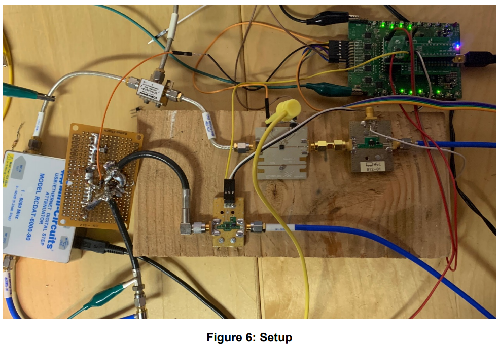
The BOM for the circuit is shown in Table 1 along with manufacturer part numbers and Digi-Key part numbers (where available).
Note: Values were copied from the Mini-Circuits data sheets for both amplifiers.
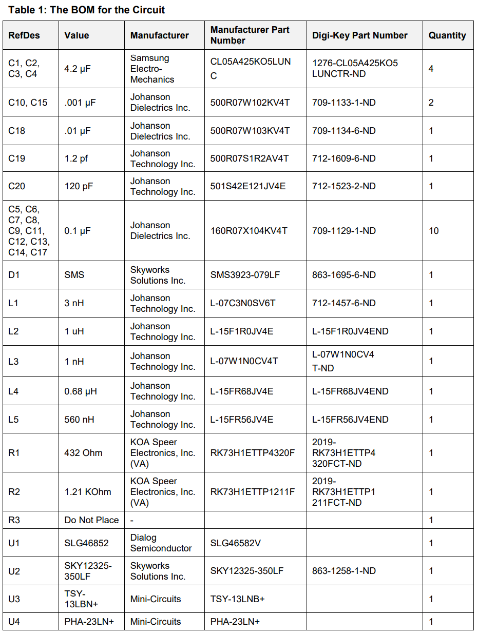
Raspberry Pi Control Software
A RaspberryPi software package has been written to allow monitor and control of the SLG46582 circuit described in this project. The software allows the RaspberryPi’s GPIO pins to interconnect with the SLG46582V. The HighPower Assert and LNA Enable functions on pins 4 and 6 have been implemented. The High Power Enabled (Pin 10), LNA Enabled (Pin 18), LDO Fault (Pin1) and Overtemp (Pin 3) flags are all monitored. This software requires the WiringPi Libraries for proper operation. Please see http://wiringpi.com for installation instructions.
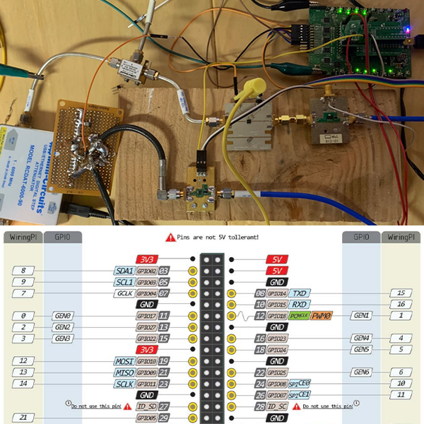
The GPIO pinout for the RaspberryPi is shown in Figure 4 below.
For our circuit, WiringPi pin 0 (GPIO17) is the HP_Enable Pin. WiringPi pin 2 (GPIO27) is the LNA_Enable pin. For the monitoring side, WiringPi pin 4 (GPIO23) is the HP_Enabled flag. WiringPi pin 5 (GPIO24) is the LNA_Enabled flag. WiringPi pin 6 (GPIO25) is the Overtemp flag. WiringPi pin 27 (GPIO16) is the LDO_Fault flag.
Measurements
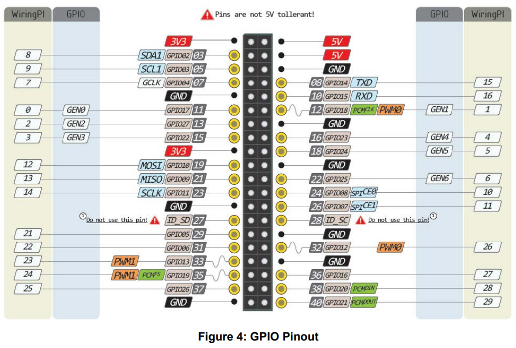
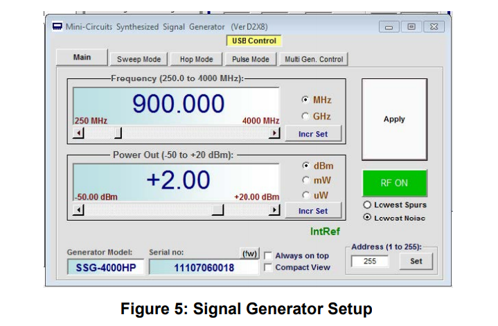
Measurements were taken using a Mini-Circuits SSG-4000HP as the signal generator (Figure 5). Power measurements were made using Mini-Circuits PWR-SEN-8GHS USB power meters. Attenuation control to simulate signal fading was made using a Mini-Circuits RCDAT-6000-90. The signal generator was set to 900 MHz and the output power to +2 dBm. Following the output of the signal generator, the RF path was split using a Mini-Circuits ZX10-2-252-S+ power splitter. One arm of the power splitter attached to the SKY12325-350LF DSA. The other arm of the power splitter was connected to the RCDAT controllable attenuator. This arm was then connected to the TSY-13LNB+ LNA. The output of the TSY-13LNB+ was connected to another Mini-Circuits PWN-SEN-8GHS power sensor. A GreenPAK Advanced evaluation board and SLG46582-DIP module were used for the bias controller emulation. A Klein Tools DVM was inserted into the supply line for the PHA-23LN+ to measure the bias current. Each RF path was measured without the circuit in place and offsets entered into the power meters to set the reference to 0 dBm. This allows us to see the gain of the RF circuits. The setup is shown in Figure 6.
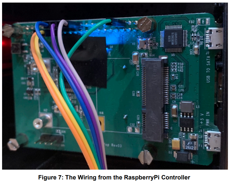
The wiring from the RaspberryPi controller is shown in Figure 7 below.
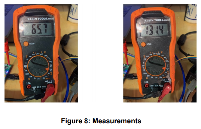
In low power mode, the PHA-23LN+ drew 65.7 mA at 3.0 V. This is slightly lower than the data sheet specification of 72.4 mA. At 5 V bias, the PHA-23LN+ drew 131.4 mA. The spec calls out 141.7 mA (see Figure 8).
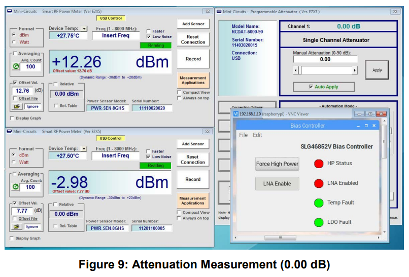
In low power mode the PHA-23LN+ output 12.24 dBm of power. The digital step attenuator has approximately 7 dB of attenuation. Since our input power is normalized to 0 dBm, this gives us approximately 19.24 dB gain. The spec sheet calls out 19.7 dB of gain at 3 V. This is close for what is really an uncalibrated setup. The LNA path is showing almost 3 dB of loss. The spec for the TSY13LNB+ in bypass mode is about 1.9 dB of loss (see Figure 9). The approximately 1 db remaining loss is due to the detector circuit (as mentioned before it is not an ideal design).
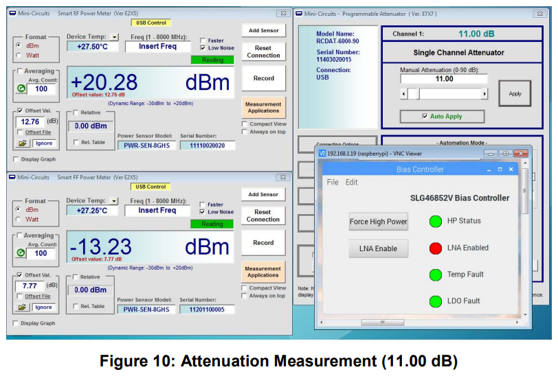
In high power mode, the PHA-23LN+ output +20.28 dBm of power. The attenuator has approximately 0.8 dB of attenuation at minimum attenuation. This equates to 21.08 dB of gain. The spec at 5 V is 21 dB. The relative improvement in signal from low power to high power, we see an improvement of 8 dB of power with at 5 V. This makes sense since the attenuator has approximately 7 dB of attenuation at low power and the PHA-23LN+ has an extra dB of gain at 5 V vs. 3 V.
These first example image shows the performance with the LNA disabled. This is the point at which the high-power mode of the circuit became enabled. 11 dB of additional attenuation has been added to the LNA path dropping the detector voltage (see Figure 10).
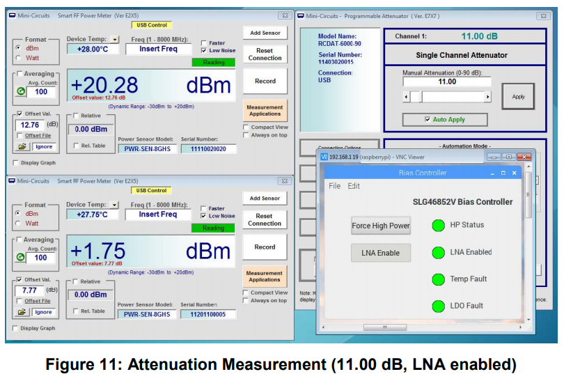
With the LNA enabled, we see the following performance at high power. The LNA is providing approximately 14.98 dB of gain. This is slightly better than the typical specification performance numbers (see Figure 11).
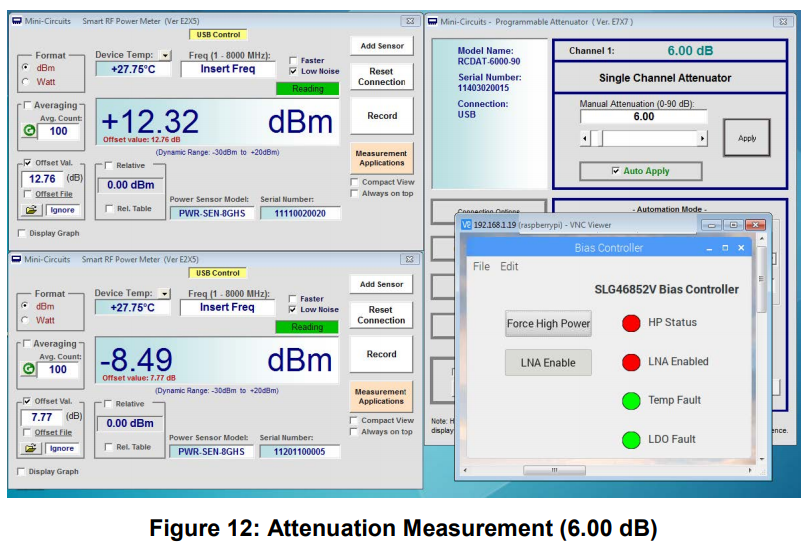
Decreasing the attenuation, the circuit shifts back to lower power mode around the 6 dB mark. There is approximately 5 dB of hysteresis in the RF power range. This has to do with the performance characteristics of the comparators in the GreenPAK IC. See Figure 12 on GreenPAK performance.
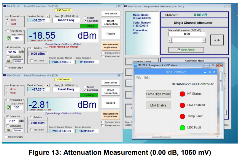
Next, as shown in Figure 13, it was desired to test the temperature monitoring performance of the SLG46582 bias controller. For this example, the Comparator3 trip level was changed from 1000 mV to 1050 mV. This equates to a temperature of about 85 °C vs 95 °C. This was done to prevent damage to the circuits but show how this safety feature performs. A heat gun was used to heat up the circuitry. As can be seen, the Temp Fault flag shows red. The DC voltage to the amplifiers was completely cut off until the circuit cooled. Once cooled, operations resumed as normal.
Further Design Considerations
GreenPAK Comparators: During attenuation testing, it was discovered that the outputs of comparators in the GreenPAK devices do not instantly switch output states (high to low or low to high) upon hitting the threshold voltage. Rather, the output voltage from the comparator begins to drop at threshold and continues dropping linearly as the input voltage continues to drop below the reference voltage. It appears the gain and loop bandwidth of the comparators are not sufficiently high to switch right at threshold or shortly lower. The same holds true as the input voltage begins to increase and rise toward the reference voltage. Using an external Vref with precision resistors to set the voltage may improve this performance. That was not done in this example. Additionally, there are no additional pins available to use external references.
Detector Design: As discussed previously, the design of the detector circuit could be improved in both sensitivity, loss and overall performance. This design was sufficient to show the performance of the circuit.
Test Equipment: The Mini-Circuits portable test equipment pieces are excellent and low cost. However, should precise measurements need to be made including possible spectral degradation at the bias cross-over point, higher performance test equipment would be needed. At this time, it is unknown what performance impact would take place with the RF signal at the transition point between bias settings. This could be explored further in depth and we welcome any feedback on this.
Higher Power RF Amplifiers: If a similar circuit is desired for amplifiers that run with higher bias current than the SLG46582 is able to provide, a similar design has been done utilizing the Dialog SLG46867V GreenPAK IC. This GreenPAK has dual 2 A Power FET switches. The circuit switches between the two power FETs to change the bias point of the amplifier. The user would need to provide their own regulated voltages for each bias state (up to 6 V max). Please contact the author if this circuit is desired.