This project illustrates how to use the SLG47004 to implement an adjustable analog filter.
Introduction
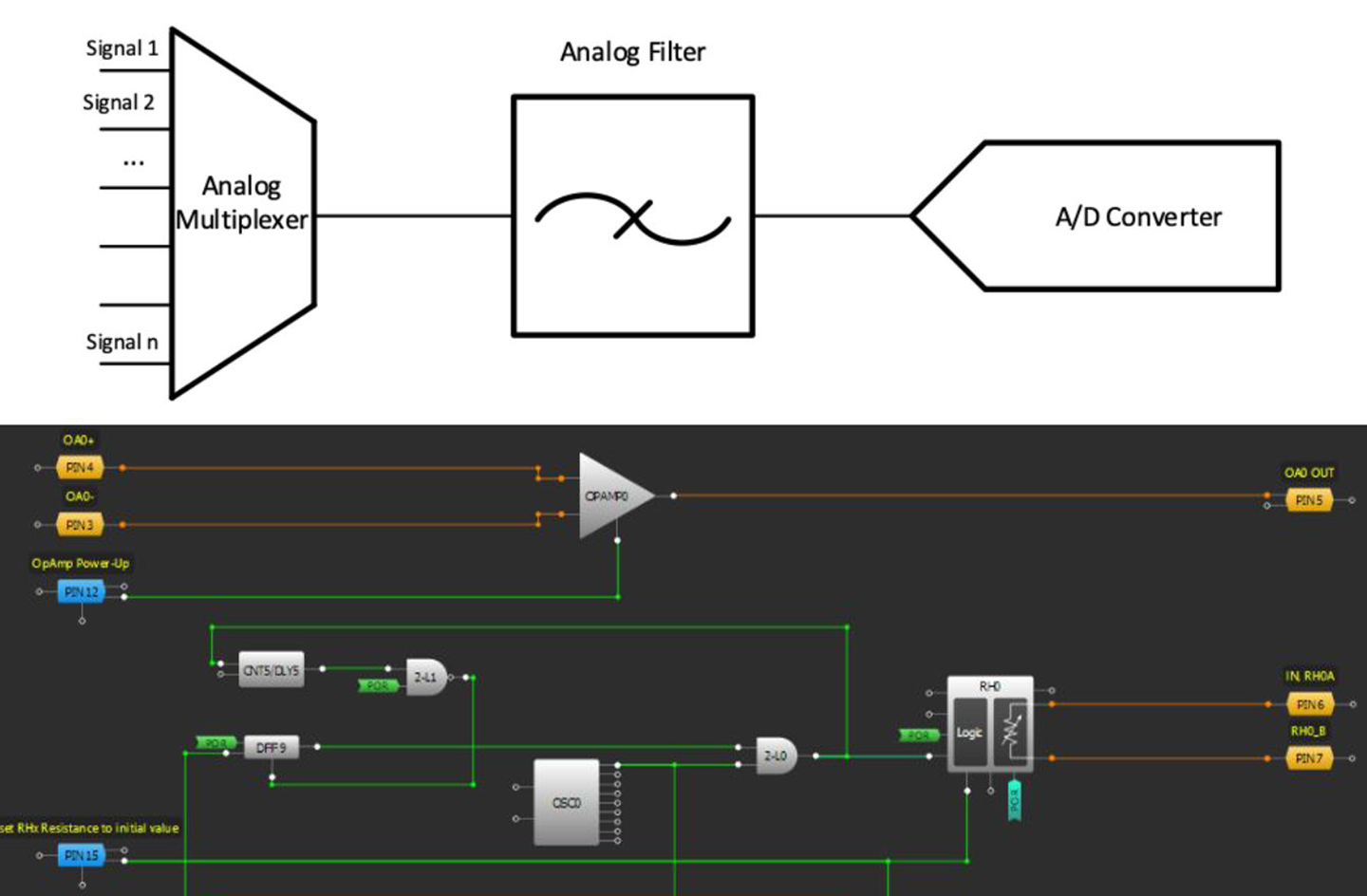
There are a variety of applications where signals from different sources (for example, sensors) are sensed with one ADC. Such systems require an analog multiplexer with analog filters for each channel, because each signal source may have its own set of filter requirements (for example, different cutoff frequencies). An alternative space-efficient and cost-efficient solution is to use one tunable analog filter for all channels (Figure 1). The SLG47004 IC solves this task perfectly.
Below we described steps needed to understand how the solution has been programmed to create the adjustable analog filter. However, if you just want to get the result of programming, download GreenPAK Designer software to view the already completed GreenPAK Design file. Plug the GreenPAK Development Kit into your computer and hit the program to design the device.
1. System Overview
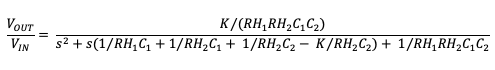
This project demonstrates the implementation of the adjustable analog filter by highlighting an example second-order, programmable, active low-pass Sallen-Key filter (Figure 2).
This filter is implemented with two resistors, two capacitors, and an operational amplifier. Two resistors in this circuit are replaced with the SLG47004 Digital Rheostats, and one of the SLG47004 operational amplifiers is used as an active element.
By adjusting two Digital Rheostats the cutoff frequency and the approximation method of this active filter can be changed. The Butterworth approximation method was used in this project. The frequency behavior of the Butterworth filter is maximally flat in the magnitude response in the passband. The rate of attenuation in the transition band is better than the Bessel filter, though not as good as the Chebyshev filter. There is no ringing in the stopband. The step response of the Butterworth filter has some overshoot and ringing in the time domain, though this is comparatively less than the Chebyshev filter.
The equation for the low-pass filter configuration on Figure 2 is:
where K = 1;
This formula can be used to calculate the appropriate resistance and capacitance. Alternatively, it is possible to determine the capacitors and resistors values using filter design tools [Analog Filter Wizard, Filter Design Tool Webpage, Analog Devices].
The capacitor values in the filter circuit are kept constant while the resistive elements are adjusted. For this project, capacitor valuse chosen are: C1 = 270 pF and C2 = 27 pF.
The SLG47004 contains two 10-bit Digital Rheostats. The full resistance for both Digital Rheostats is 100 kΩ. The range of digital code that corresponds to the rheostat resistance is from 0 to 1023 (1024 taps). Code 0 corresponds to the minimum resistance between the RHx_A and RHx_B terminals. As the code value increases, the resistance between the RHx_A and RHx_B terminals monotonically increases. Consequently, when the code value decreases, the resistance between the RH0_A and RH0_B terminals decreases as well. The voltage on any rheostat pin can be in the range from AGND to VDDA, and can be dynamically changed during operation.
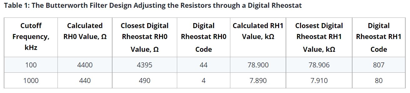
The values calculated for this filter design are summarized in Table 1. This table also includes the closest resistance values for RH0 and RH1 along with the digital program code.
2. Functional Block Architecture
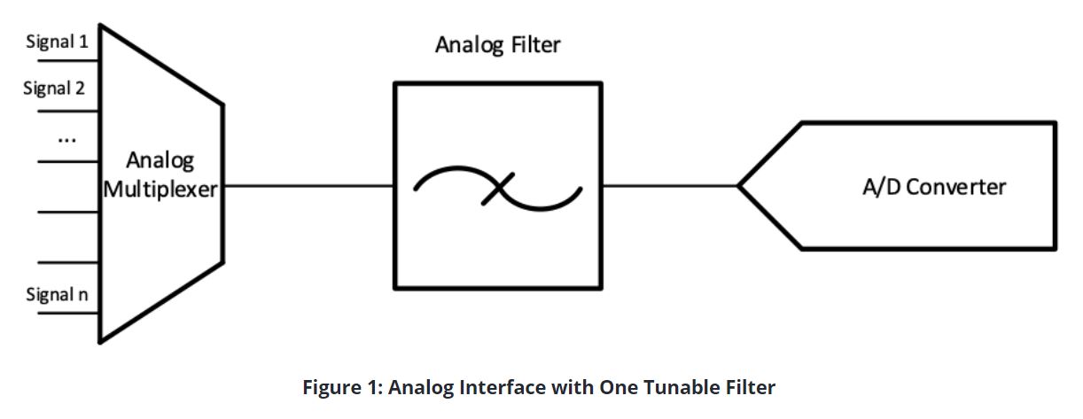
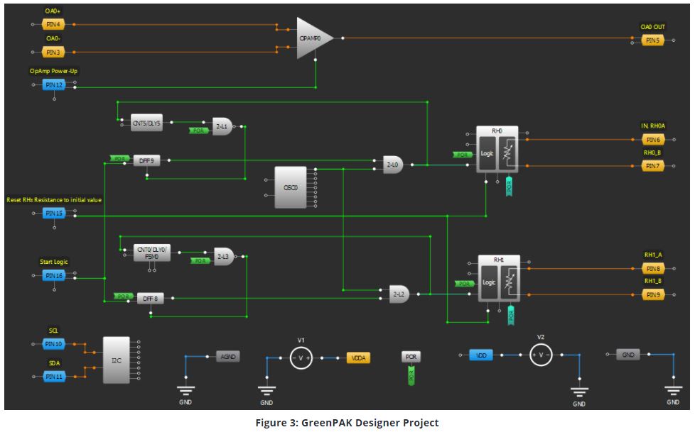
Figure 3 shows the internal design of the project in GreenPAK Designer software.
2.1. Setting Rheostat Data
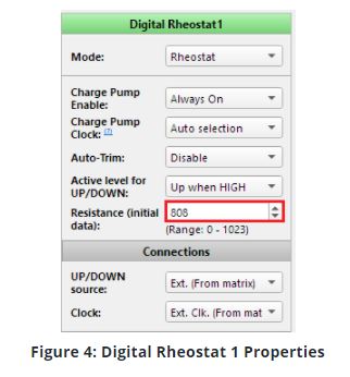
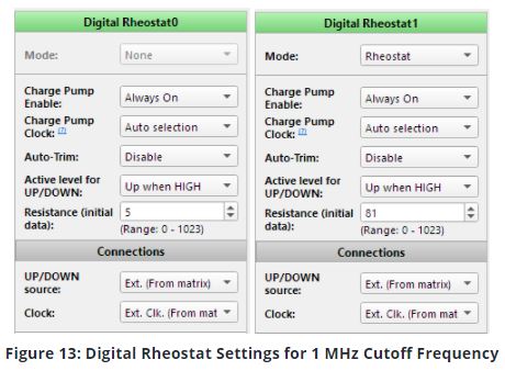
Both rheostats allow setting "Resistance (Initial data)" in their properties and thus setting the desired filter's cutoff frequency (Figure 4).
2.2. Changing Rheostat Data
There are two ways to change Digital Rheostats value: using I2C, and using internal logic.
2.2.1. Changing Rheostat Value via I2C
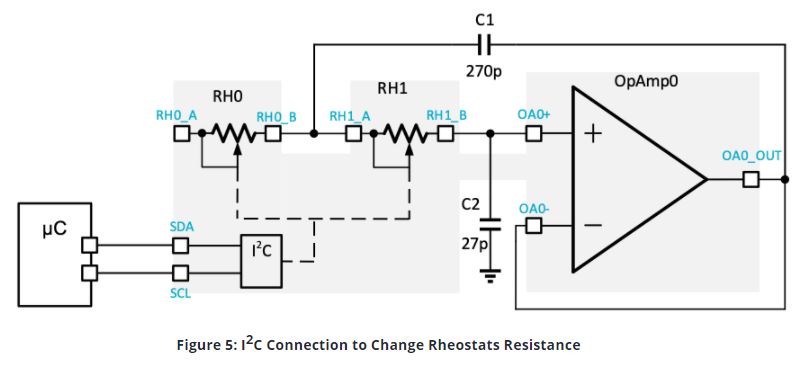
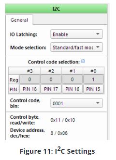
The SLG47004 has an I2C macrocell, which allows reading and writing data to Digital Rheostats (Figure 5). The rheostats resistance data is stored in the registers [C0, C1] for RH0 and [D0, D1] for RH1. The I2C master can write data to these registers and thus can adjust the cutoff frequency of the filter according to the digital code in Table 1. Note that to read the rheostat data, the I2C master should read the registers [C2, C3], [D2, D3].
2.2.2. Changing Rheostat Value via Internal Logic
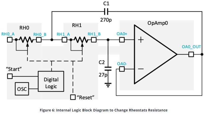
Adjusting the cutoff frequency by I2C is a simple and convenient method, but it requires an I2C master. An alternative method can be implemented with two pins and internal logic (Figure 6).
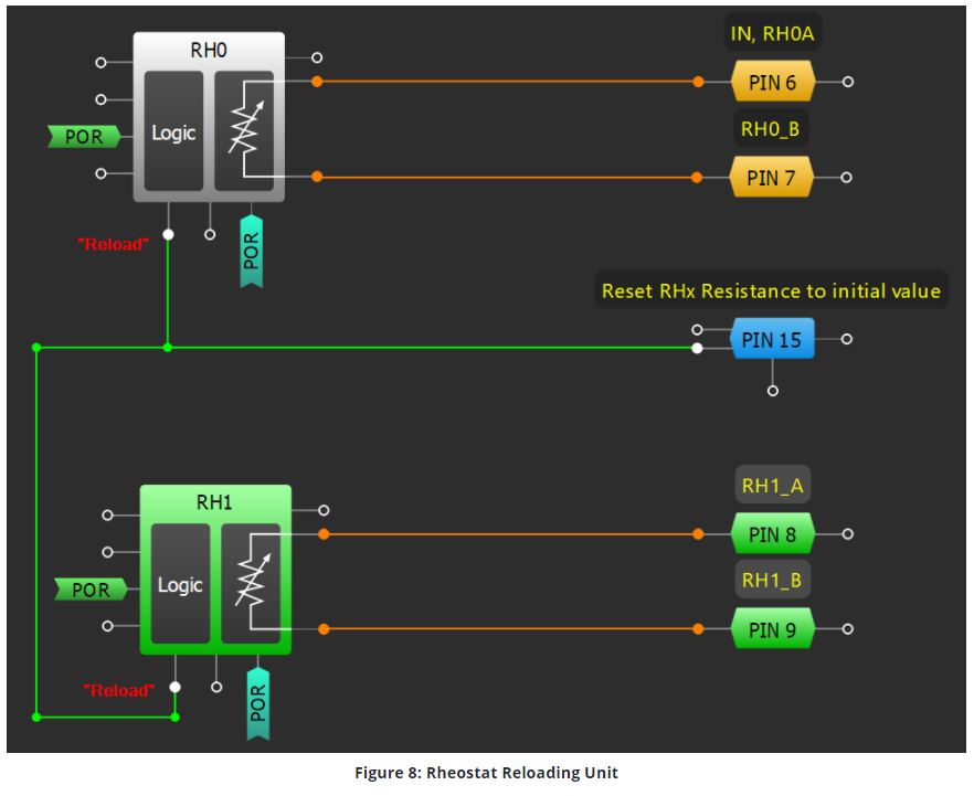
A High level signal on the Start (Pin 16) and Reset (Pin 15) pins allows switching between two different frequencies. When the rheostat's initial value is set to 100 kHz cutoff frequency, the High level signal on Pin16 starts changing this frequency to 1 MHz (Figure 7). The High level signal on Pin15 resets the frequency again to 100 kHz (Figure 8).
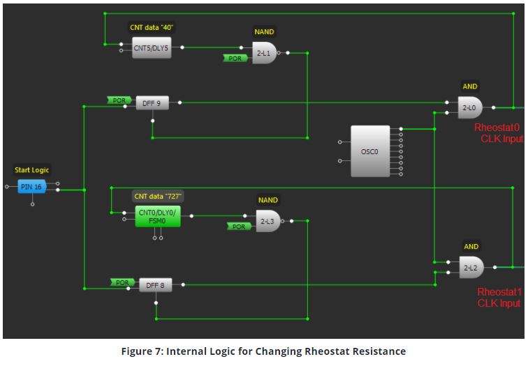
To detail this behavior further, for 1 MHz cutoff frequency RH0 resistance is 488 Ω (code 4) and RH1 is 7.910 kΩ (code 80). To change the frequency to 100 kHz the RH0 resistance = 4.395 kΩ (code 44) and RH1 resistance = 78.906 kΩ (code 807). So, for RH0 the digital code value must be increased by 40 and for RH1 by 727. To increase the resistance in the rheostat's settings "Active level for UP/DOWN" must be set to "Up when High".
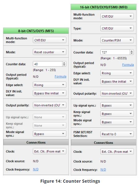
8-bit and 16-bit Counters can be configured to provide the necessary number of clock pulses from the oscillator to the rheostats. 8-bit Counter data must be set to "40" and 16-bit Counter to "727".
СNTs stop is provided by the internal logic (Figure 7). When "Start Logic" signal goes High, DFFs will trigger on its rising edge. A High level on DFFs outputs will cause a clock signal on LUT0 and LUT2 outputs. After that, Counters values start going down and when they reach "0" a High level will appear at LUT1 and LUT3 inputs respectively. As these LUTs are NAND gates, a High level of signals on their inputs will reset the corresponding flip-flop and will stop counting.
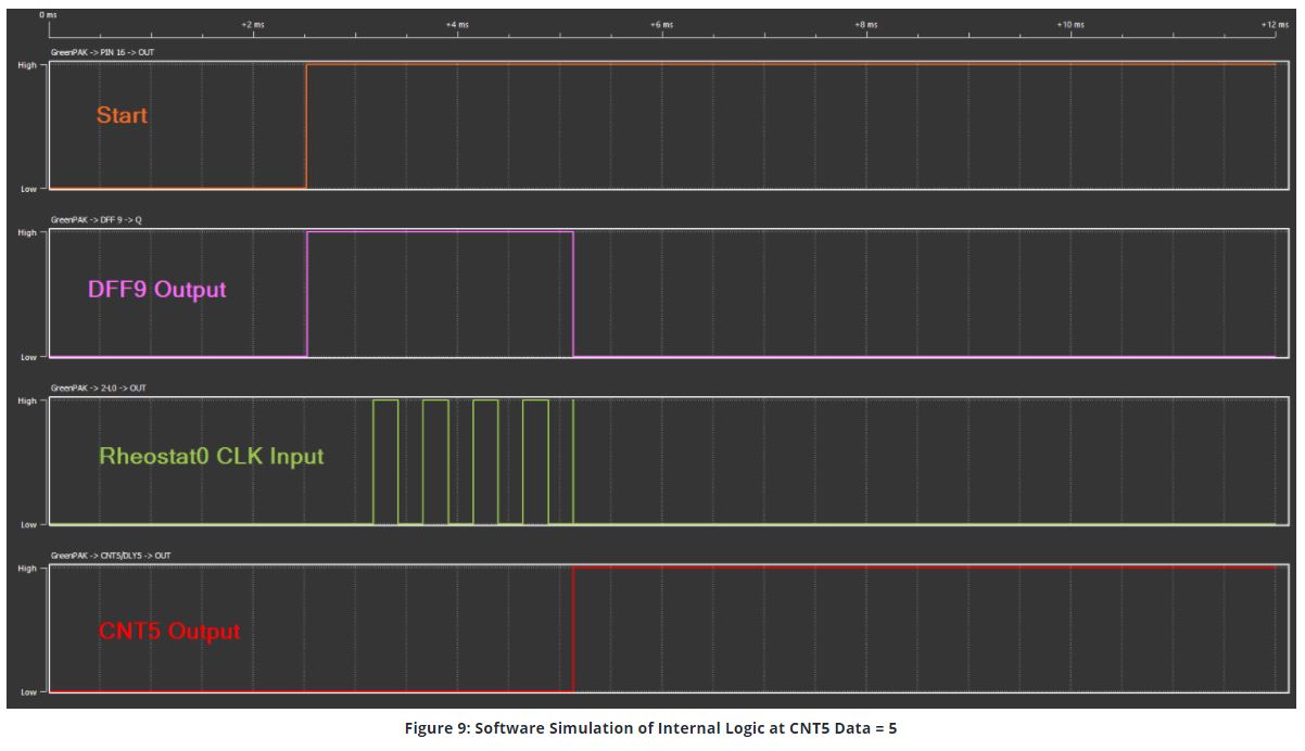
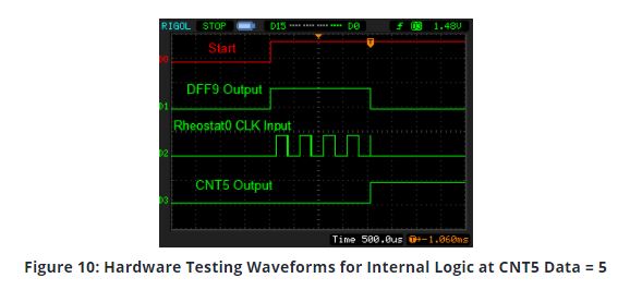
Software simulation results for this internal logic are shown in Figure 9. For hardware testing refer to Figure 10.
For resetting the cutoff frequency Pin15 works as a Digital Input and is connected to "Reload" input of the rheostats. When Reload signal goes High, the rheostat value stored in the MTP NVM will be loaded into the rheostat (Register and Counter) overwriting any current setting. For the normal rheostat operation "FIFO nReset" input should have a logic High level (Figure 7).
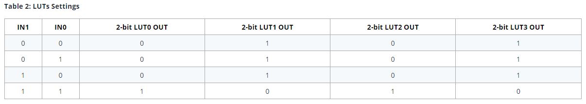
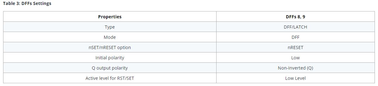
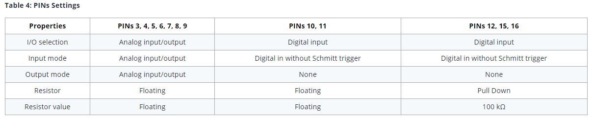
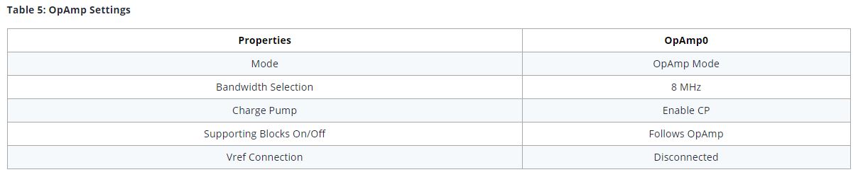
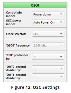
2.3. Macrocells Settings
2.4. Software Simulation
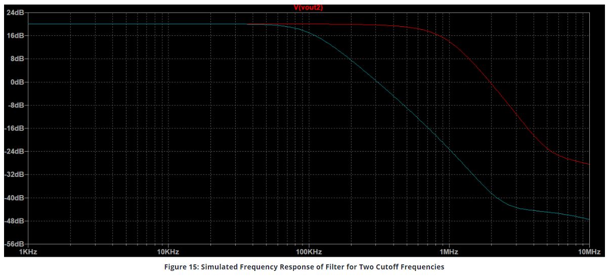
The frequency response of the second-order, active low-pass Sallen-Key filter ( for 100 kHz and 1 MHz corner cutoff frequencies) is shown in Figure 15.
2.5. Hardware Testing
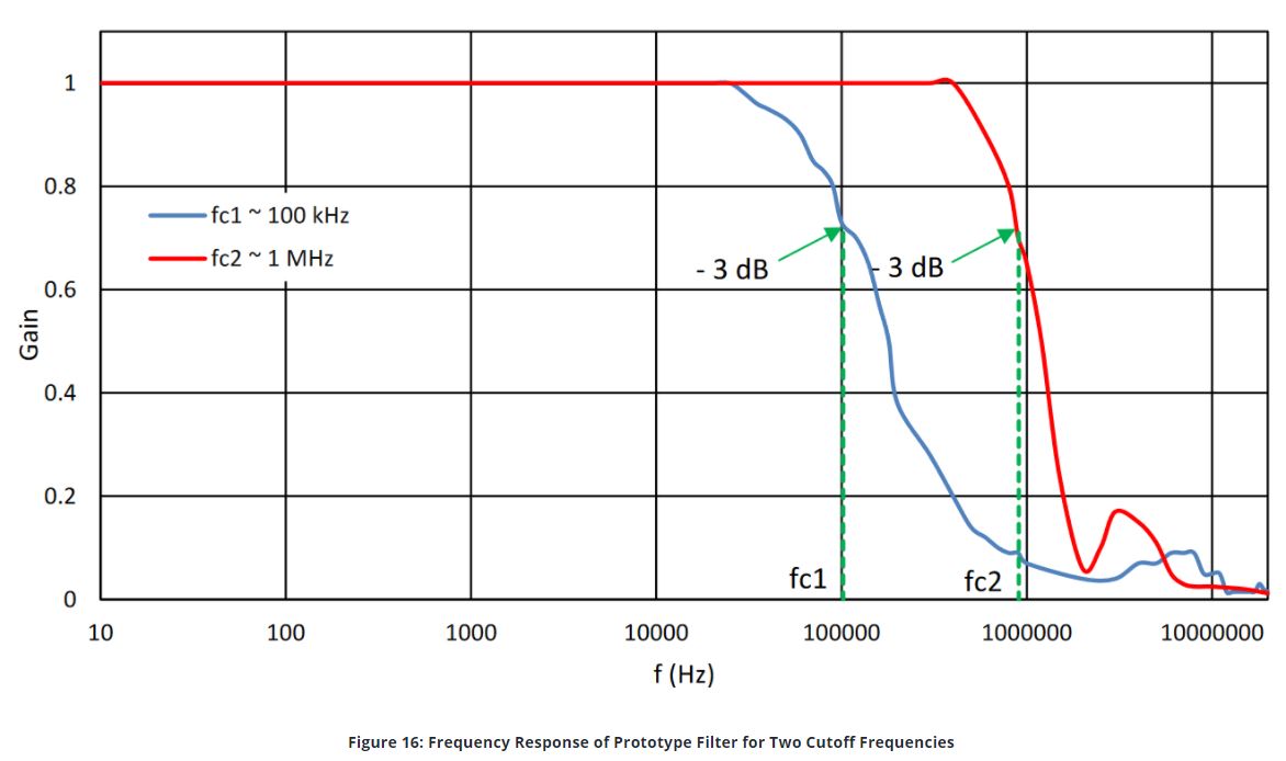
Results of prototype testing for both cutoff frequencies are shown in Figure 16.
Conclusions
The SLG47004 has the necessary internal resources to implement advanced analog features. This project illustrates how to implement an adjustable analog filter as a functional replacement of multiple standard products. Using one tunable analog filter for different cutoff frequencies provides a more flexible, cost-efficient solution that yields a smaller PCB footprint and lower power consumption. Due to the configurable nature of the SLG47004, this project's approach can be easily expanded for augmented functionality, such as adjusting other filter requirements like the filter approximation method.