Check out how to create a compact yet capable Li-Ion battery charger
Below we described steps needed to understand how the solution has been programmed to create a rapid charger. However, if you just want to get the result of programming, download GreenPAK™ software to view the already completed GreenPAK Design File. Plug the GreenPAK Development Kit to your computer and hit the program to design the solution.
Introduction
There are many off-the-shelf ICs available for charging Li-Ion batteries. In this project, we present a LiIon charger design based on a GreenPAK mixed-signal IC and a GreenFET integrated power switch from Dialog Semiconductor. There are some advantages to use the GreenPAK approach. For one, we may integrate the solution with other circuit functions – related or unrelated – in the same IC. This helps in reducing the overall footprint in an application. Secondly, we can customize the solution by incorporating context-specific control mechanisms in the same GreenPAK chip; for example, in some contexts the battery need not always be charged to full capacity, and the design can be tailored to terminate suitably early so as to prolong battery life. Thirdly, the inherent design flexibility can be exploited – the power supply used for supplying the bulk charge current can be from a different domain than the supply used to power the GreenPAK chip. All of these features are especially useful in systems powered by renewable energy or harvested energy where the charging source may have varying characteristics, and there may sometimes be a tradeoff between using the source for powering a load or charging a battery.
It is useful to understand the Li-ion charging process with reference to the lead-acid charging process. The traditional lead-acid battery charge cycle has Bulk, Absorb (CV), and Float (CV) phases. (The Bulk phase is often called the Constant Current (CC) phase but this is misleading because the battery need not be charged with a constant current per se.) It is important to complete the charge cycle by running it though all three phases to maintain capacity and prolong life. However, Li-Ion battery charging differs from lead-acid charging in the following aspects:
There is no Float phase – charging current must drop to zero once Absorption is complete; completion of Absorption is signaled by the charge current dropping to a suitably low value that is typically taken to be 0.05 C or 0.1 C.
Deeply discharged Li-Ion batteries (below an open-circuit voltage of 2.5 V) need a trickle charge of a few tens of mA to make them ready for the Bulk phase
Note that the Absorb phase of Li-Ion batteries is often incorrectly called the Float phase. Also, note that the Trickle phase of Li-ion is quite different from the Trickle phase of lead-acid batteries! More information on Li-Ion charging is available at “BU-409: Charging Lithium-ion”, Battery University, 2017-05-09.
This means we need to deal with two threshold voltages: the “Deeply discharged” threshold and the “Absorb Voltage” threshold. Additionally, we need a current threshold to detect when the current during Absorb has dropped to the charge termination threshold of 0.05C or 0.1C. The next section describes the broad strategies we may adopt for dealing with these.
Broad Design Strategy
One way to implement the design is to choose a GreenPAK chip such as the SLG46533V that has at least 3 ACMPs in it so that we can configure things to detect the voltage thresholds as well as the current threshold (by using a small resistor). This would require an external GreenFET.
Another approach is to use a GreenPAK that has a built-in power FET, such as the SLG46116/7V. However, the latter has only 2 ACMPs which we may use for the detection of the two voltage thresholds. To be able to detect the current threshold, we adopt a pulsed battery charge approach, where the current pulse magnitude stays constant but the duty cycle is varied so as to control the average current through the battery. This is considered a good approach for Li-Ion cells [“Charging protocols for lithium-ion batteries and their impact on cycle life—An experimental study with different 18650 high-power cells”, Keil P. and Jossen A., Journal of Energy Storage 6 (2016)] and is in fact used by some commercially available off-the-shelf Li-Ion charger ICs. The current threshold detection then amounts to detecting when the duty cycle has fallen below a predetermined threshold value. This allows us to use the SLG46116V with very few additional external components to give us a highly compact yet full-featured Li-Ion rapid charging solution. (In passing we note that the SLG46116V is more appropriate here than the SLG46117V which is almost identical except for the presence of a discharge resistor on the output of the latter, which we do not require).
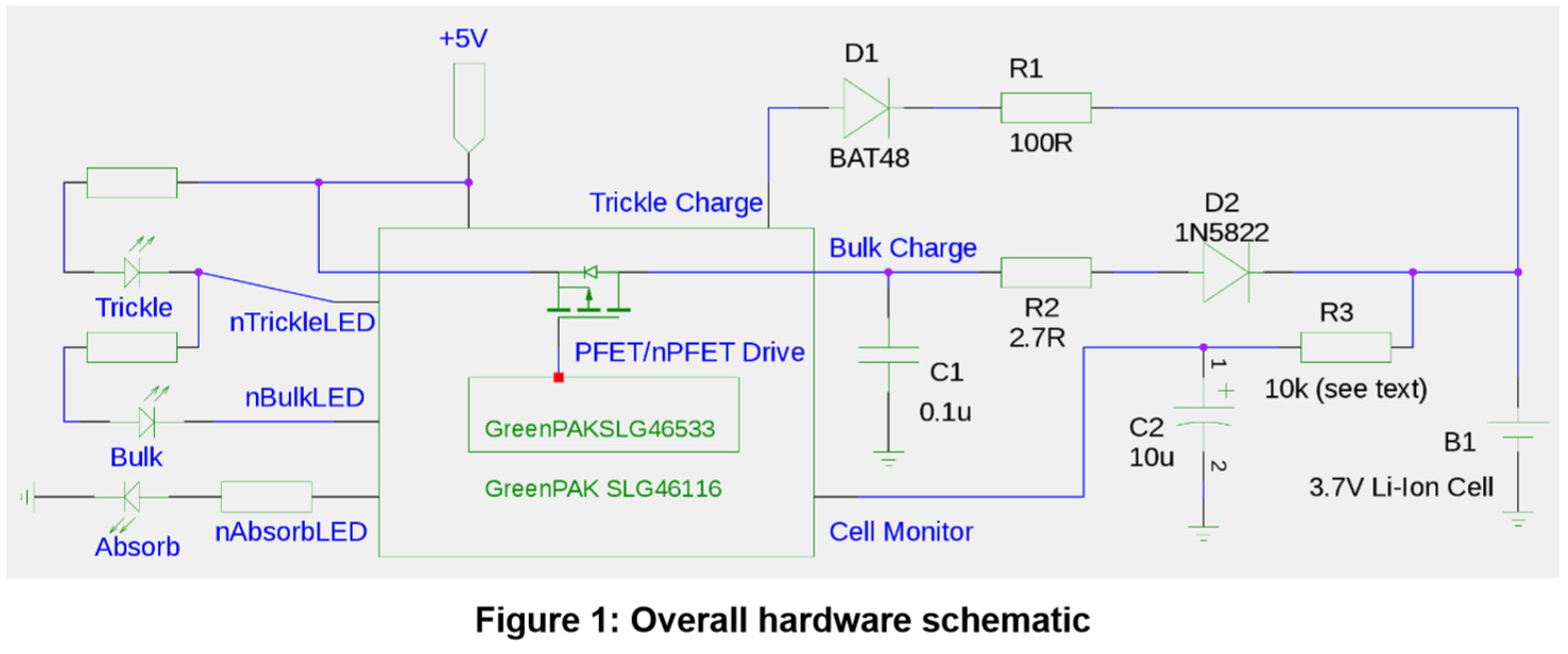
The overall schematic is shown in Figure 1. We have indicated the possibilities with the SLG46533V (smaller box) as well as SLG46116V. With the former, the smaller box is the GreenPAK, and the PFET taken to represent an external GreenFET.
The battery's bulk charge current is determined by R2 and can go up to 1A with the SLG46116V's integrated PFET and up to 2A with GreenFETs such as the SLG59M1641V. If an external GreenFET without integrated discharge resistor is used, D2 can be eliminated as the GreenFET features reverse voltage protection. In cases where the charge circuit is powered by a wall adapter with a built-in current limit that is acceptable for the battery, it is possible to eliminate R2 (i.e., replace it with a short). Note that with the simple resistive control of bulk current, the bulk current will decrease as the battery charges. With R2=2.7 ohms and D2 shorted, at 2.5V the charge current will be about 0.9A, this current will drop to about 0.6A when the battery voltage has climbed to 4V. Trickle charge for batteries below 2.5V is governed by R1 and can be set to about 20-35mA which can be handled comfortably by an open-drain PMOS GPIO pin. This trickle current is a steady DC for safety reasons (since a deeply discharged battery may not be ready where the current pulse magnitude stays constant but the duty cycle is varied so as to control the average to take large current pulses). The system is powered off 5V.
R3 and C2 form a lowpass filter at the Cell Monitor input to filter out noise and ripple from the PWM waveform. There is also another purpose that R3 serves. By increasing R3, the Absorb voltage threshold also increases due to the finite input impedance of ACMP0 (about 1M with a gain of 0.25). With the values shown, the threshold was about 4.06V which may be increased up to 4.2V for Li-Ion cells depending on their precise cell chemistry (the manufacturer's datasheet must be consulted to avoid charging the battery to unsafe levels).
Also provided are outputs to be wired to LED indicators. There are three such outputs – nTrickleLED, nBulkLED, and the AbsorbLED. The first two are low when in Trickle and Bulk state respectively. The AbsorbLED flashes once in 2.5 seconds when in Absorb state and goes high when the charge terminates. When these outputs are wired in the manner shown, only one LED is on at any time to indicate the appropriate state. Curiously enough, many sophisticated off-the-shelf charger ICs usually do not provide LED outputs to clearly indicate the three states of charging!
This design does not monitor cell temperature.
Realization in the GreenPAK Designer
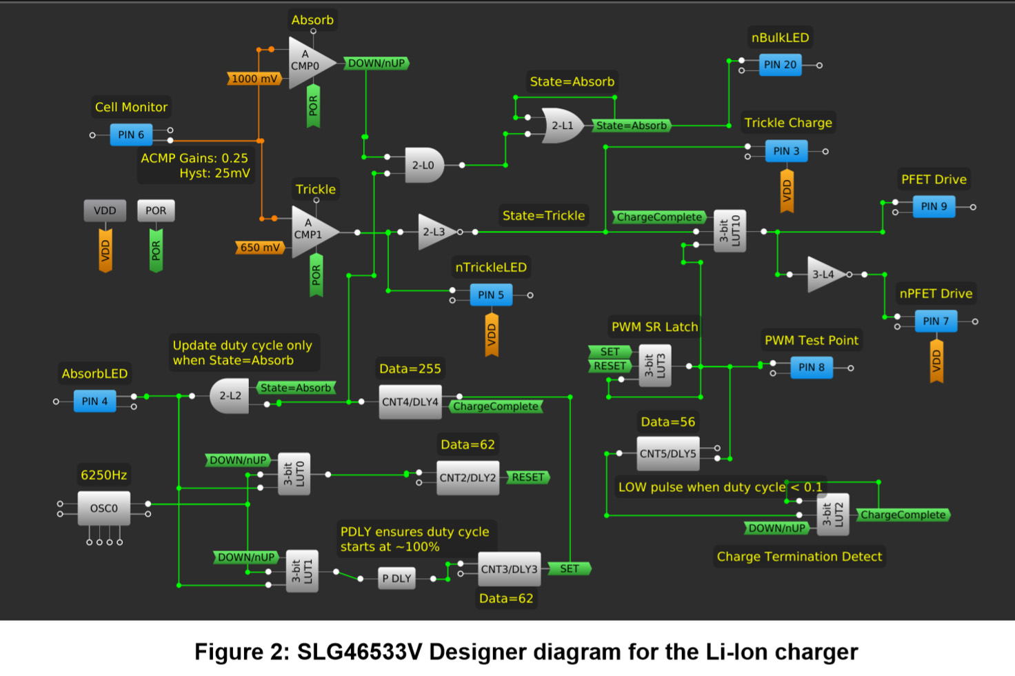
Figure 2 shows the design realized using SLG46533V. While this design uses an external PFET, all the blocks used are available in the SLG46116V which allows for easy porting to the latter.
We now explain how the design strategy is realized in the Designer.
PWM Operation. The 25KHz output of the OSC block, divided by 4 to yield 6250Hz, is used for the PWM signal generation in the manner described in Application Notes AN-1117 and AN-1122 – albeit with some minor modifications to suit the present context – so we will only provide a brief summary of the operation here and refer the reader to the detail in those Notes. The reader may also refer to the timing diagrams in Figure 3 to aid understanding.
The CNT2 and CNT3 blocks, with Data=62, generate SET and RESET pulses every 62 clock pulses which feed the SR Latch LUT10 to generate a rectangular PWM waveform; a SET causes the output of LUT10 to go high and a RESET causes it to go low. The period of the PWM waveform is the clock frequency divided by 62, which in this case is 100Hz. When the pulse width (duty cycle) needs to be increased, the DOWN/nUP signal goes low, and this causes the SET signal to occur earlier, thereby increasing the duty cycle. Conversely, when the DOWN/nUP line goes high, the RESET signal occurs earlier, causing a reduction in the duty cycle. The DOWN/nUP signal is derived from ACMP0 which monitors the battery voltage. The purpose of CNT4 is to specify a PWM duty cycle update frequency that is slower than the rate of the SET/RESET pulses. In the present context, we want updates that are slow enough to allow the battery voltage to settle down, yet fast enough to prevent overcharging. Therefore we set CNT4's Data to 255 which makes the updates happen approximately once every 2.5 seconds. What this means is that if a fully-charged battery is placed into the charger, the bulk current will start out at 1A, and monotonically drop till the charge terminates in at most 2.5x56 seconds = 140 seconds. If however the battery is not fully charged and has just entered the Absorption phase, it will be seen that the charger takes several tens of minutes (depending on its mAH capacity) before it terminates.
For more detail, on the working of the basic PWM engine, the reader may refer to AN-1117 and AN-1122.
Summary of charging algorithm. If the battery voltage is below 2.5V when the charge cycle begins, ACMP1 turns on to signal the start of the Trickle phase and drives a small direct current of about 2030mA into the battery while simultaneously ensuring the PWM output is gated off. As soon as the battery crosses 2.5V, it is ready for the high-current bulk charge phase and the PWM output comes on. When the bulk charging process starts, we want the PWM duty cycle to begin at nearly 100% and stay there till the Absorb state is reached. To ensure this we insert PDLY before CNT3. The effect of this is to delay the SET pulse at the PWM SR Latch LUT10 and make it appear “just after” the RESET pulse so the latch is in a HIGH state most of the time, corresponding to a duty cycle close to 100%. As long as the battery is not in the Absorb state, the PWM updation via CNT4 is turned off by the AND gate L2 so that the duty cycle is held constant at the nearly-100% value.
The entry of the battery into the Absorb state is signaled at the moment that its voltage crosses ACMP0's threshold (typically 4.1V for a 3.7V Li-Ion battery) for the first time. OR gate L1 then latches to signal that the battery is in the Absorb state. During emulation, it was observed that ACMP0's output momentarily goes high at startup irrespective of the input voltage. To prevent L1 from latching from such spurious pulses, AND gate L0 was introduced so that the output of ACMP0 is polled only when a pulse emerges from CNT4. This offers a delay of about 2.5 seconds from startup. Once the Absorb state is entered, AND gate L2 starts letting the update pulses through. At this point, since ACMP0's output is high, the updates cause a slight reduction of the duty cycle. Thereafter the duty cycle is adjusted constantly to maintain the battery voltage between the hysteresis limits of ACMP0. As the battery charges, this required duty cycle becomes lower and lower, till it finally drops below the predecided threshold value (here 10%) and the charging process is terminated. The realization of the termination logic is explained in more detail later.
The external PFET drive output is provided on two outputs. The output nPFET Drive is opposite in polarity to the PFET drive output; the appropriate output must be selected depending on the GreenFET used. For example, the SLG59M1641V (a fast GreenFET without discharge resistor) turns on with a low applied to its gate and so we use nPFET Drive. (L4 is not required if the design is implemented in a GreenPAK with integrated PFET such as the SLG46116V.) In selecting a GreenFET it is important to ensure that its rise/fall times are small enough to not distort the PWM pulse at duty cycles of ~ 10% so that there is an accurate correlation between duty cycle and average charge current.
The PWM duty cycle is monitored at pin 8 and all it requires is an analog voltmeter: at 100% the voltage will read about 4.7V, and as the duty cycle drops so does the analog voltmeter reading till charge termination happens at about 0.45V as shown in the photograph alongside (full-scale is 2.5V).
Charge termination. Suppose we have decided that the charge termination condition is for the duty cycle to drop below 10% during Absorb. The PWM waveform has as many clock pulses as the Data field of CNT2/CNT3, which means we want to sense a PWM pulse that is shorter than 10% of this Data field, or, equivalently, a PWM low that is longer than 90% of the Data value. Since Data=62 for CNT2/3, the PWM period is 62 pulses long. We set the Data=56 for DLY5 which is configured to delay both edges. Therefore, DLY5 acts as a filter, and as soon as the PWM's low pulse is longer than 56 clock pulses, the delayed falling edge appears on the output. At this point LUT2 checks if ACMP0's output is high; if yes it latches into a high state causing charge cycle termination by turning off the PWM output. At this point the duty cycle is frozen because a RESET is applied to CNT4; this allows the terminating duty cycle to be measured at leisure. To restart charging, power must be cycled.
To make the charger settle into a low-power state upon charge termination, the ChargeComplete net may be connected to OSC0's PWR DOWN pin.
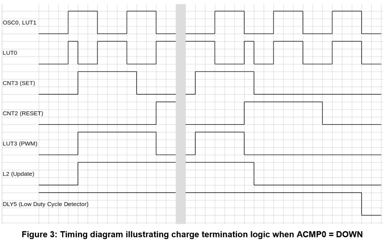
The timing diagram illustrates this process in detail when the output of ACMP0 is high (DOWN). The first SET pulse in Figure 3 from CNT3 has triggered an update pulse from L2. The LUT0 pulse gets split into extra pulses that cause the second RESET pulse from CNT2 to occur earlier in relation to the SET pulse. Therefore, we see that the PWM pulse has shortened in width and therefore that the duty cycle has decreased. This has caused a low pulse from the duty cycle detector DLY5.
There is a small subtlety here. Note that the low duty cycle detection has not come “at the same time” as the update pulse – it has come after a delay of more than one PWM cycle. It is quite possible that ACMP0 has “changed its mind” and briefly toggled to a low (nUP) state at the time that DLY5 has output a low pulse before again switching to the DOWN state. This is especially likely when there is noise or ripple at the ACMP0 input. When this happens, the visible effect is usually that the duty cycle continues to decrease beyond the charge termination threshold because DLY5 has not “caught” ACMP0 when it is DOWN. If this happens a few times then the PWM engine underflows and the duty cycle may shoot back to 100%. This is why we choose to delay both edges from DLY5 rather than only the falling edge; this allows the output of DLY5 to stay low long enough for it to be coincident with a DOWN from ACMP0 and ensure more reliable charge termination.
Test Results and Notes
Lab tests were performed on the SLG46533V version of the design and a 3.7V 18650 battery. Just as the present design does not have any check for testing for underflow of the duty cycle, it does not have an explicit check for duty cycle overflow – i.e., a situation where ACMP0 outputs an nUP when the duty cycle is already near 100%, causing the next SET pulse to appear “just before” the RESET pulse which would result in the duty cycle attempting to increase beyond 100% and therefore dropping to nearly zero. Since the duty cycle updates start only when the Absorb state is triggered, and since this state is triggered only when ACMP0 has output a DOWN, the above situation is normally not expected to happen. However, it is possible for such a situation to be triggered by the ripple level at the Cell Monitor pin, which is why we have a lowpass filter consisting of R3 and C2 at the Cell Monitor input. Values shown were found to work satisfactorily during tests. If the problem nevertheless manifests itself, higher values of R3 and C2 can be experimented with. When increasing the value of R3 remember that the ACMPs have an input impedance of about 1MΩ and gain error of about 3% at a gain of 0.25x. Therefore, the IN- voltage must be suitably lowered for higher values of R3 and the circuit recalibrated.
With the schematic values shown and the ACMP0 IN- voltage set to 1000mV, absorption kicked in at 4.07V and was maintained between 4.03 and 4.07V till charge termination. The charge current at the start of absorption was 0.5A essentially limited by the wall-wart (a 5V USB charger). The charge termination duty cycle was set to 10% which led to an average termination current of 0.5A.
While testing the design we do not normally have the patience to charge a battery all the way up from, say, 3V or 3.5V because it could involve waiting for over half an hour. It is often more practical to rapidly discharge a fully charged battery till it is just below the Absorb threshold, and then put it in to charge mode so that the wait time can be reduced to a few minutes! This can lead to some unexpected situations, such as the charger entering the Absorb phase sooner than expected, or the duty cycle overflowing past 100%. To avoid such situations while testing, it is advisable, after rapidly discharging the battery, to wait for a couple of minutes for the battery to “settle down.” Then verify that upon connecting to the charger, the Absorb phase does not come on for at least 2 minutes.
Conclusion and Extensions
This project presented a compact yet capable Li-Ion battery charger. There is considerable scope for experimentation with this design – for example, we may try different PWM frequencies and see what frequency leads to the best results for different Li-Ion chemistries. While this is a subject of ongoing research it is difficult to find definitive answers to this question in the trade literature. More complex designs would include temperature monitoring and the ability to vary charge current and termination threshold with battery temperature to ensure optimum charging and battery life. An even more sophisticated “parametric” charger could be designed that would include an I2C interface to allow some degree of user control over charger parameters such as the termination voltage with battery chemistry so that the charger acquires more universality and can be adapted to newer Li-Ion chemistries as they are released into the market.