Draw a .PCB four documents contained in
First create a new PCB project
File-> New-> Project-> PCBProject
1. Schematic file name.SchDoc
File->new->Schmatic
2. Principle library file name.SchLib
File->New->Library->Schematic Library
3. Package library file name.PcbLib
File->New->Library->PCB Library
4.PCB file name.PcbDoc
File->New->PCB
principle library file:
draw all the symbols (device inside the schematic)
system comes with
draw their own;
Schematic file:
drawing schematic diagram;
wire, network label, other electrical components;
Package library file:
the shape and electrical characteristics of all devices on the PCB board;
PCB file: the
last file sent to the manufacturer;
Two: unit conversion
1mil = 0.0254 mm
100mil = 2.54mm
1inch = 1000mil = 25.4 mm
3. Some commonly used shortcut keys
ZA display all the things currently drawn
DO change principle paper size normal use C
PP place pin
X, Y mirror operation can make the component about the X axis or Y axis symmetry
ED delete
TA unified named
Tools-> Footprint manager View package, add package (schematic)
Tools->New Component Create a new component (principal library file)
Tab Modify property
Ctrl + M Measure distance
Ctrl + G Modify the display grid, pay attention to the multiple relationship (very important)
EJC lookup Components
Ctrl + shift + Spaces form corners
Tools->New Blank Component Create a new package of own paintings (package library files)
Toola->Component Wizard Guided package drawings (system comes with)
Q Switch unit
TDR Last copper after error detection
G Modify the capture grid, modify the
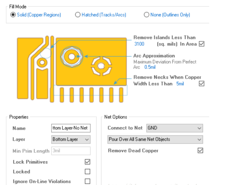
DR setting rules (PCB file) when the movement is inconvenient
Report->Project Report->Bill of Materials (PCB file)
keypad * Punch (PCB file)
Four few notes and techniques.
Should Component schematic library files when drawing at the center;
the cross pin is placed when to put the outside;
schematic network reference numerals corresponding to the wireless connection;
encapsulation library file can be provided by a reference line The way to draw the package diagram;
when many of the same components are packaged, you can change the component to the package by right-clicking the component -> Find similar objects->Description into the same->Component Designator;
delete the PCB of the PCB file. ->Filter Then enter Iskeepoutlayer;
put a lay (package library file) attribute laye to multi-layer;
in the package library file, set the coordinate origin to Pin_1 or center->
Edit->set after encapsulating a file Reference->pin_1 or center (very important)
power line generally choose 30mil, right-click new rule in Design->rules->width ->net->VCC (for example)
pin pad, border with silkscreen layer (package library file)
the PCB power supply wiring drawing portion preferentially
found then directly introduced directly modify Design-> import (PCB schematic drawing file error or an error when the package drawing wiring)