An analog switch is a switch that uses the characteristics of JFET or MOS to control the signal path.
An analog switch is a switch that uses the characteristics of JFET or MOS to control the signal path, and is mainly used to complete the switching function of signal link connection or disconnection. Because of its low power consumption, fast speed, no mechanical contacts, small size and long service life, it has been widely used in various automatic control systems and electronic digital products.
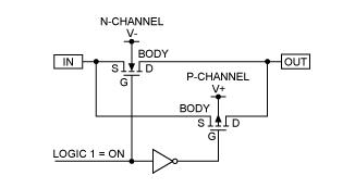
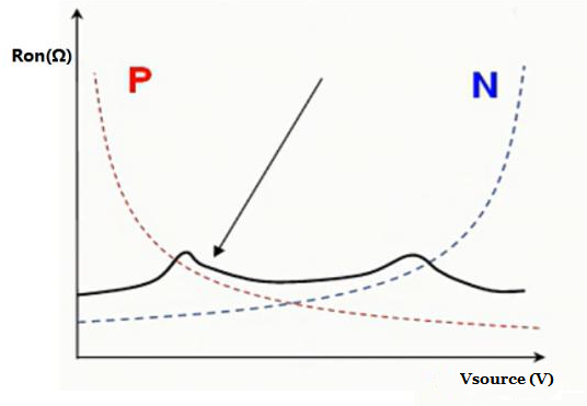
The structure of the traditional CMOS process analog switch is shown in Figure 1. Connecting NMOS and PMOS in parallel allows signals to pass equally smoothly in both directions. The gate is used to control the turn-on and turn-off of the switch. NMOS turns on when Vgs is positive, and turns off when Vgs is negative, and PMOS does the opposite. Due to the different characteristics of PMOS and NMOS, the switch composed of them has the characteristics shown in the figure below. The amount of signal current carried between NMOS and PMOS is determined by the ratio of input to output voltage. Since the switch does not have the problem of selecting the direction of current flow, there is no distinction between input and output. The two MOSFETs are turned on or off under the control of internal inverting and non-inverting logic. The advantage of CMOS switches is the rail-to-rail dynamic range, bidirectional operation, and the on-resistance remains unchanged when the input voltage changes.
Static parameters (on-resistance, leakage current, logic control trigger level): ① on-resistance RON, the difference of on-resistance between different channels RON, the flatness of on-resistance RFLAT(ON).
On-resistance will cause signal loss, especially when the load in series with the switch is low impedance. In the application, a switch with an appropriate on-resistance should be selected according to the actual situation. Special attention should be paid to the fact that the resistance of the on-resistance is directly related to the power supply voltage. Generally, the higher the power supply voltage, the smaller the on-resistance.
The on-resistance of the NMOS tube is small when the signal is relatively low, while the on-resistance of the PMOS tube is small when the input signal is high. After the two resistors are connected in parallel, they are relatively low in the effective range of the entire signal.
Leakage Current: A switch in an ideal state requires zero resistance in the on-state, and the on-resistance in the off state tends to be infinite, and the leakage current is zero; in fact, the switch is in a high-impedance state when it is off, and the leakage current is zero. The current is not zero, and the conventional CMOS leakage current is about 1nA. When the switch is off, the leakage current will flow into the load, causing additional errors. If the internal resistance of the signal source is very high and the transmission signal is DC, it is particularly necessary to consider the leakage current of the analog switch. Generally, the smaller the leakage current, the better.
It should be noted that if the impedance of the front-end circuit through the analog switch is large, the effect of leakage current cannot be ignored. If the impedance of the front-end circuit is small, the effect of on-resistance will be greater.
Logic control trigger level VIH, VIL. VIH can be recognized by the analog switch as the minimum level of logic high; VIL can be recognized by the analog switch as the maximum voltage of logic low.